You've probably encountered this situation: a meticulously designed circuit board becomes unusable due to a hard-to-detect cold solder joint, requiring hours of debugging.
We must understand that soldering is the foundation of hardware manufacturing, and its quality directly determines success or failure. This article will systematically explain how to achieve "error-free" soldering.
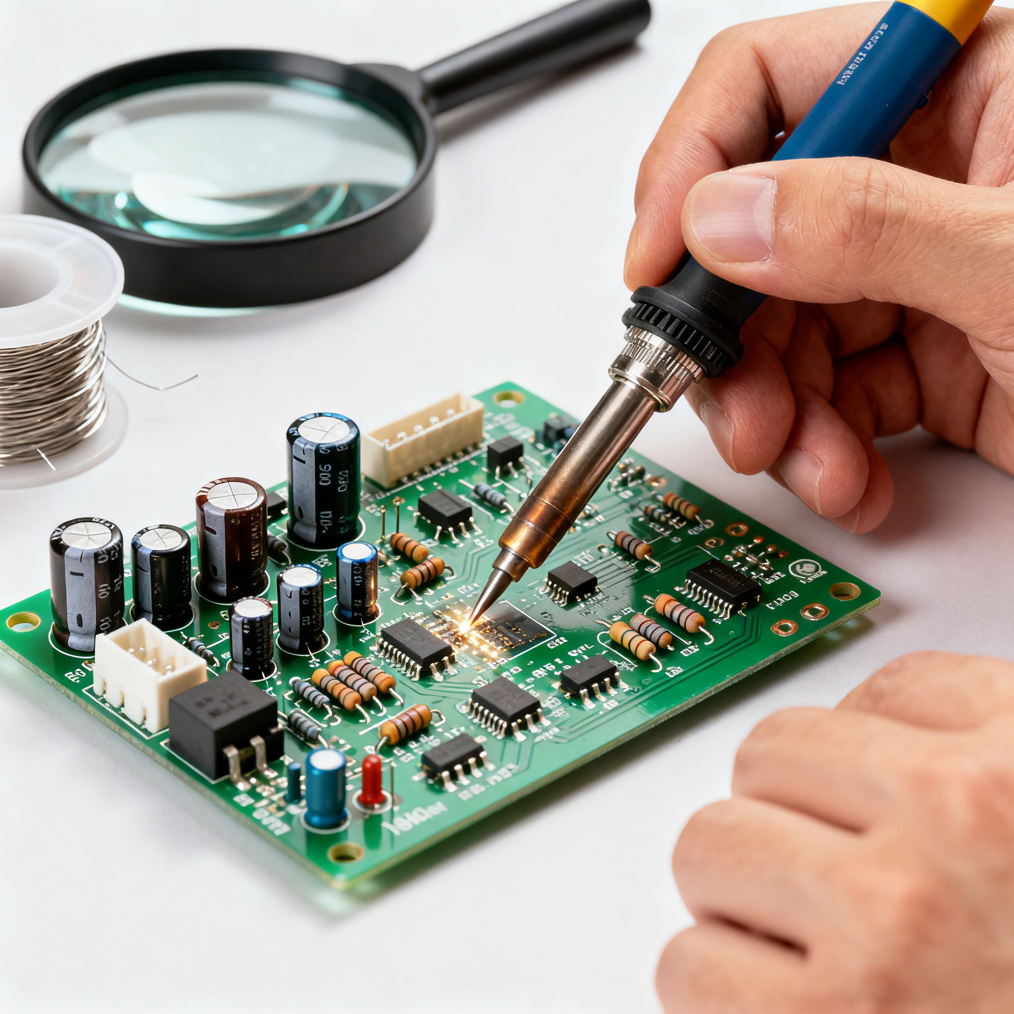
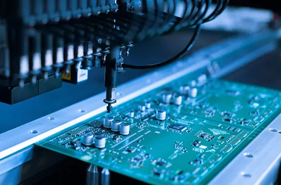
First, let's briefly understand what soldering is. Soldering a PCB circuit board refers to the process of fixing electronic components onto a printed circuit board (PCB) using soldering techniques. This process typically uses a soldering iron (or other heating tools) to melt solder and connect the component leads to the pads on the circuit board, thus forming a stable electrical connection.Soldering generally has two methods: manual soldering and automated soldering (such as reflow soldering and wave soldering). Manual soldering is suitable for small batches or repairs, while automated soldering is suitable for large-scale production.

This article will focus on manual soldering, explaining how to achieve error-free PCB circuit board soldering.
4. Solder Joint Inspection:
5. Cleaning Solder Joints:
6. Post-Soldering Inspection:
7. Circuit Testing:
1. Cold Solder Joint
Symptoms: The solder joint surface is rough, cracked, or the connection is not firm, leading to a broken circuit or poor contact.
Causes: Insufficient soldering temperature, the solder not fully melted, or the soldering time is too short.
Inspection Method: Inspect the solder joint with a magnifying glass. Cold solder joints usually appear irregular or cracked, and the solder surface is not smooth.
Solution:
1)Reheat the solder joint to ensure the solder is completely melted.
2)If the solder joint surface is cracked, remove the existing solder, clean the pads, and resolder.
2. Short Circuit (Solder Bridge)
Symptoms: Excess solder connects two adjacent solder joints, causing a short circuit.
Causes: Excess solder was not removed in time during soldering, or solder flowed into inappropriate places during soldering.
Inspection Method: Carefully observe the circuit board with a magnifying glass, especially between the leads of small components, for any unwanted solder bridging.
Solutions:
1)Use desoldering wick or a desoldering pump to remove excess solder.
2)Use a soldering iron to heat the short-circuited area and quickly remove excess solder, ensuring there is no electrical connection between the two pins.
3. Loose Solder:
Symptoms: Loose solder joints or component leads may not be firmly secured, potentially leading to poor contact or component detachment.
Causes: Insufficient solder or insufficient soldering time, preventing the solder from fully melting.
Check Method: Gently touch the solder joint or component lead to check for looseness.
Solution:
1)Reheat the solder joint to ensure the solder is fully melted.
2)Add an appropriate amount of solder to ensure a firm solder joint.
4. Excessive Solder:
Symptoms: Excessive solder on the solder joint, forming rounded bumps, may cause poor pin contact or short circuits.
Causes: Applying too much solder during soldering.
Check Method: Inspect each solder joint for obvious solder buildup or excessive solder.
Solution: Use desoldering wick or a desoldering pump to remove excess solder.
5. Overheating Damage
Symptoms: Components burn out, PCB is damaged, or solder pads detach.
Causes: Soldering iron temperature is too high, soldering time is too long, or too much heat is applied during soldering.
Inspection Method: Inspect the damaged components and solder pads. Overheating damage may present with obvious burn marks or surface damage.
Solutions:
1)Lower the soldering iron temperature to avoid damaging components with excessive heat.
2)Shorten the heating time each time to avoid prolonged heating of components.
3)Use a hot air gun for hot air soldering to avoid direct heating of components.
6. Incorrect Component Orientation
Symptoms: Components (such as diodes, electrolytic capacitors, integrated circuits, etc.) are incorrectly oriented, causing the circuit to malfunction.
Causes: The polarity or orientation of the component was not carefully checked.
Inspection Method: Check whether the markings on the component (such as the bar and polarity symbol for diodes, and the markings for capacitors) match the markings on the PCB.
Solutions:
1)Reinstall the component, ensuring its correct orientation.
2)If already soldered, reheat the solder joints, remove the component, and reinstall it.
7. Pad Lifting
Symptom: The pad separates from the PCB substrate, causing unstable soldering.
Cause: Excessive soldering temperature or use of too much solder causes the pad to detach.
Inspection Method: Use a magnifying glass to inspect the pads for separation from the PCB.
Solution:
1)If a pad has detached, stop soldering immediately to avoid damaging other components.
2) The pad can be repaired using jumper wires or conductive adhesive.
8. Poor Flux Residue
Symptom: Flux residue remains on the PCB surface after soldering, which may cause corrosion or short circuits.
Cause: Residual flux was not cleaned promptly after soldering.
Inspection Method: Use a magnifying glass to inspect the solder joints and PCB surface for residual flux.
Solution:
1) Clean the PCB surface with alcohol and a non-woven cloth to remove residual flux.
2) If acidic flux was used, special care must be taken to clean it thoroughly.
9. Component Overheating
Symptoms: During soldering, some components overheat, leading to burnout or performance degradation.
Causes: Soldering time is too long, or the heating area is inappropriate.
Inspection Method: Check if the heated components are overheated or deformed.
Solutions:
1)Shorten the heating time for each soldering attempt.
2) Use a hot air gun instead of directly using a soldering iron to avoid component overheating.
If your circuit board doesn't work properly after soldering, besides the soldering issues mentioned above such as cold solder joints and short circuits, you also need to review the PCB itself. Please double-check that your board dimensions and layout are correct, especially whether the component packages match the actual components. If you made last-minute design changes, review the precautions in "How to Change PCB Size in Ultiboard".
Additionally, if you used an internal PCB printer, you also need to check if the printed traces are clear and free of breaks. We discussed in detail how to achieve optimal printing results and avoid such problems in "What Makes Our PCB Printer the Perfect Choice?". A multi-faceted check is essential to accurately pinpoint the root cause of the error. "
Mastering these core principles and techniques will give you a solid foundation for achieving error-free soldering. Remember, reliable soldering is the ultimate bridge between innovative design and stable products—it ensures that every meticulously designed PCB is perfectly activated and performs to its full potential.
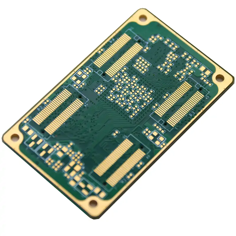
Of course, perfect soldering begins with a perfect PCB.
As your trusted electronics manufacturing partner, Hongrong (Shenzhen) Electronics Co., Ltd. understands this deeply. We offer much more than a Gerber file or a bare board. From the moment you complete your design, our one-stop PCB fabrication and assembly service is ready. From "idea" to "product," Hongrong Electronics aims to be your smoothest link. Whether it's providing high-quality bare PCBs or undertaking complete end-to-end manufacturing, we are here to help.


Please contact us to experience the difference with high quality of HongRong (shenzhen) Electronics Co.,Ltd.