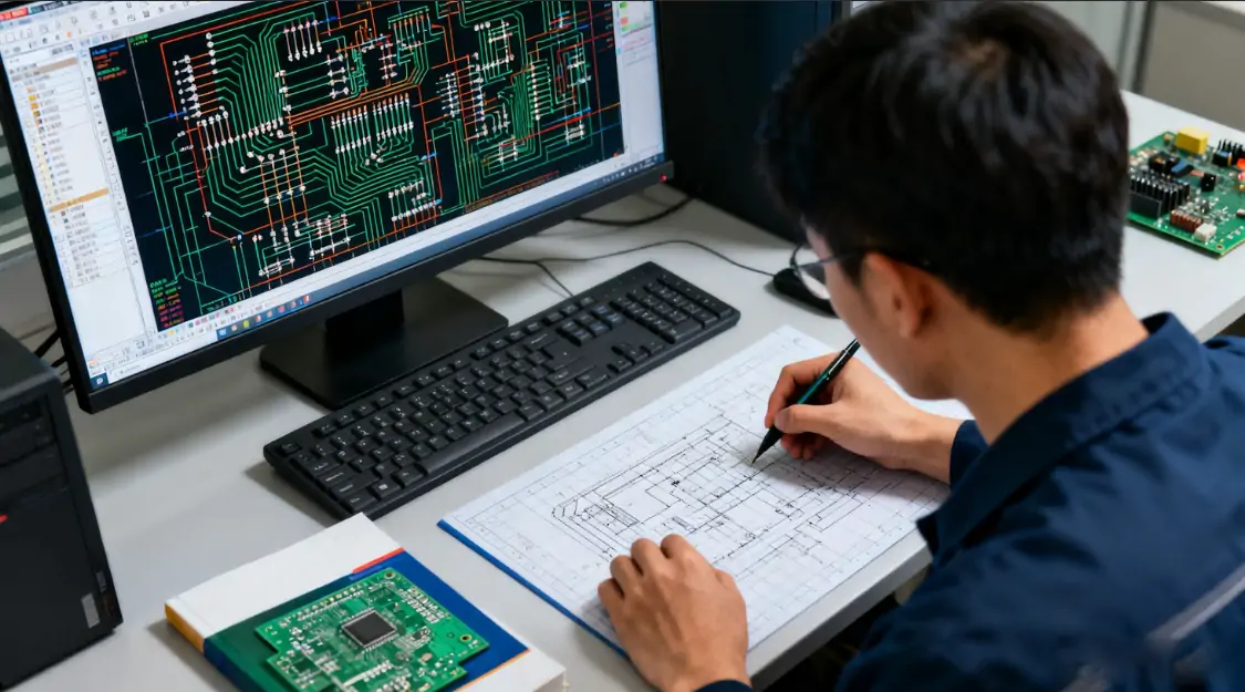
Designing a multi-layer PCB requires detailed planning, technical precision, and a strong understanding of electrical and mechanical performance. This is common sense in today's electronic machines, where size and functionality matter. Multi-layer printed circuit boards are used in smartphones, computers, medical devices, automobiles, and aerospace systems, offering increased signal transfer speeds, reduced interference, and improved signal integrity. To achieve such success, the PCB design must be executed properly, including the selection of materials, layering, wiring configuration, and effective thermal control. Modern high-performance electronic devices cannot do without design optimisation, since every facet of performance contributes to overall performance, reliability, and manufacturing efficiency.
Understanding Multi-Layer PCB
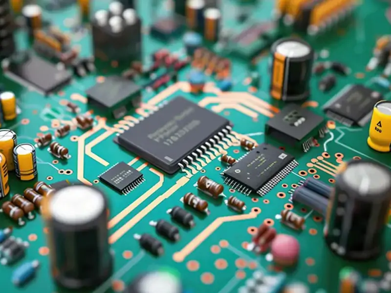
Before designing multilayer PCBs, it is essential to understand how the boards are configured and the benefits they offer. Multi-layer PCBs are constructed by crimping several conductive and insulating layers to create a small and rigid base that can be densely connected with a circuit and still maintain signal integrity.
Structure and Function of Multi-Layer PCBs
Multilayer PCBs are typically stacked with alternating layers of copper (conductor) and dielectric (insulator). Depending on the circuit's complexity, the number of layers may range from 4 to 16 layers or more. Due to noise reduction and stable voltage supply throughout the system, ground and power planes are usually added.
Example Stack-up Table:
|
Layer
|
Function
|
Description
|
|
Top Layer
|
Signal
|
Used for component placement and routing
|
|
Layer 2
|
Ground
|
Reduces EMI and improves signal return
|
|
Layer 3
|
Power
|
Distributes voltage evenly
|
|
Bottom Layer
|
Signal
|
Secondary routing layer
|
Advantages of Multi-Layer PCBs
- Realisation of miniaturisation and high-density circuits
- Improved signal integrity and reduced interference
- Stable electrical performance in high-speed circuits
- Ideal for PCB design of compact and complex electronics
Material Selection for Multi-Layer PCBs
Material selection is the foundation of every multi-layer PCB design. Suitable materials directly affect the durability, signal integrity, heat resistance and environmental stress resistance of the substrate. To achieve both stability and productivity by selecting the right laminate and copper thickness.
Common Material Types
- FR4: Most common, cost-effective and used in general-purpose electronics.
- High-frequency laminates: Designed for microwave and RF PCB designs that require minimal signal loss.
- Polyimide: Highly heat-resistant, ideal for flexible or rigid flex multilayer PCBs.
- Rogers Material: Used in aerospace and 5G systems for superior signal integrity at high frequencies.
Factors to Consider When Selecting Materials
When selecting materials, engineers must consider the balance between performance and cost. The dielectric constant, thermal expansion coefficient, and moisture absorption are essential factors. For example, materials with a low dielectric factor contribute to maintaining impedance control and improving signal integrity. Similarly, excellent thermal stability ensures that the substrate can respond to various environmental conditions without peeling or distortion.
Layer Stack-Up in Multi-Layer PCB
The multilayer structure defines the placement of conductive and insulating layers. In multi-layer PCB design, the multilayer structure determines noise control, EMI shield, and wiring efficiency. Improper layering can lead to signal loss, interference, and manufacturing issues.
Typical Stack-Up Examples
Four-layer multilayer PCBs typically consist of two signal layers, a ground plane, and a power plane placed between them, which enhances shielding and current flow. With more advanced PCB designs, 6 or 8 layers of laminates increase control. The separation of analogue and digital signals for each additional layer improves signal quality and reduces crosstalk.
Key Design Guidelines
- Adjacent ground and power planes to enhance decoupling effects.
- A symmetrical laminated structure is adopted to prevent warping during manufacturing.
- Assign dedicated layers for high-speed signal wiring.
- Maintains the dielectric thickness uniformly for impedance control.
Signal Integrity in Multi-Layer PCB Design
Signal quality ensures that the electrical signal is transmitted without distortion. Improper multilayer PCB design can cause signal reflection, timing errors, and data loss. Consistency of impedance, differential pair wiring and crosstalk reduction are key to signal stability.
Techniques to Maintain Signal Integrity
- Adopt control impedance for high-speed tracing.
- Match the differential pair length of the data line.
- Avoid unnecessary via on critical signal paths.
- Use a ground plane to provide a continuous return journey.
Importance of Impedance Control
Impedance control is one of the most essential elements in multi-layer PCB design. Impedance inconsistencies can cause signal reflection and energy loss, especially at high frequencies. Designers maintain consistent impedance across the board by carefully defining trace width, interval and dielectric thickness. This ensures accurate data transmission and ensures signal integrity throughout the PCB.
Thermal Management in Multi-Layer PCBs
Overheating can damage delicate components and reduce the reliability of boards. Thus, multi-layer PCB designers should consider using suitable thermal management techniques to maintain performance and extend the life.
Techniques for Better Thermal Control
Heat generated by components such as processors and power supply ICs must be dissipated efficiently using thermal vias or copper piles. By placing the heat source evenly in each layer, hotspot generation can be prevented. Designers can also improve both mechanical stability and signal integrity by placing copper planes that uniformly diffuse heat.
Thermal Management Solutions
- Use a thicker copper layer to increase thermal conductivity.
- Add multiple thermal vias under the heat sink.
- Ensure direct heat transfer pathways for high heat generation components.
- Apply thermal conductors between chips and PCB layers.
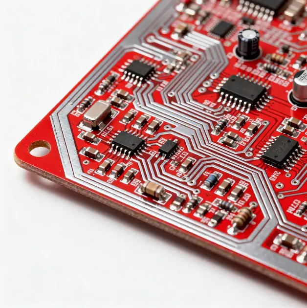
Component Placement and Routing in Multi-Layer PCB
Proper part placement and wiring improve board reliability, manufacturing and signal integrity. This is one of the most practical aspects of multi-layer PCB design, where layout decisions have a direct impact on performance.
Placement Principles
Critical components, such as microcontrollers, oscillators, and memory chips, are placed in proximity to each other to minimise latency. High-speed parts are placed near connectors and control impedance lines. On the other hand, power supply parts need to be placed at the end to reduce noise interference to different layers.
Routing Guidelines
- Keep signal tracing as short and linear as possible.
- Avoid bending 90 degrees and use a 45-degree angle instead.
- Separate analogue and digital wiring for interference prevention.
- Unify the trace width to ensure a uniform current path.
Design for Manufacturability (DFM)
Superior multi-layer PCB design not only provides excellent performance but also simplifies the manufacturing process. Manufacturing design (DFM) ensures that PCBs can be manufactured efficiently without defects or high costs.
DFM Guidelines
At the design stage, manufacturing capacity should always be taken into consideration. For example, spacing and drill sizes must meet manufacturer restrictions, and unnecessary layers should be avoided to reduce costs. By following DFM rules, you can reduce rework, improve yield, and maintain reliable signal integrity for each production lot.
DFM Best Practices
- Wire width and spacing are subject to manufacturer design limitations.
- Avoid complex via structures that increase costs.
- Ensure the clearance of the copper foil area and the substrate end.
- Ensure that all files comply with Gerber format standards for accurate manufacturing.
Testing and Validation in Multi-Layer PCB
Testing ensures that multi-layer PCBs meet electrical and mechanical standards. The final verification step before mass production ensures long-term signal integrity and functionality of the signal.
Types of PCB Testing
- Electrical Testing: Detects short circuits and disconnects.
- Functional Testing: Make sure the board works as expected.
- Thermal Testing: Check for temperature-related stress problems.
- Impedance Testing: Ensure high-speed tracing consistency.
Benefits of Proper Testing
Thorough testing prevents high-cost failure after assembly. Verify that wiring, materials and layers function in a real-world environment. The multi-layer PCB design also confirms that the timing and strength of signals are consistently maintained in all layers, reducing the risk of device failure and improving overall reliability.
Trusted Partner for Reliable Multi-Layer PCB Design and Manufacturing
To achieve optimal performance and quality in multi-layer PCB design, it is crucial to select the proper manufacturer. HRPCBA (HongRong Shenzhen Electronics Co., Ltd.) is an amalgamation of over 25 years of experience in the field, offering precise and dependable multi-layer PCB solutions through optimised technologies. In PCB production, we ensure that all substrates are fully assembled and tested to meet international standards. One-stop service guarantees high signal integrity, effective production and uniform outputs to every project, whether it is a prototype or mass production.
Why choose HRPCBA:
- More than 25 years of industry experience in ISO and UL certification
- One-stop service for design, manufacturing and assembly
- Strict quality control based on IPC-A-600F standards
- Advanced SMT/DIP/AOI production line for precision processing
- Short delivery time, flexible lot size, global delivery support
Conclusion
Multi-layer PCB designs are sensitive to striking the right balance of electrical, mechanical, and thermal parameters to achieve maximum performance. In the choice of material and its layering, as well as wiring technology and signal integrity maintenance, every phase of PCB design has a determinative effect on the success of the final product. To ensure that every board functions effectively in its actual environment, engineers must consider productivity, testing, and cost efficiency. With precise planning and quality assurance, the properly designed multilayer PCBs ensure stable performance, long service life and compliance with global industrial standards for modern electronic systems.


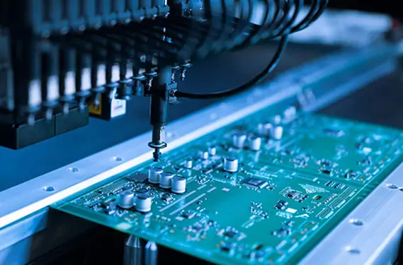
 PCB AssemblyHRPCBA is a PCBA China manufacturer offering high-quality PCB assembly services with full-process support, from design to assembly and testing.
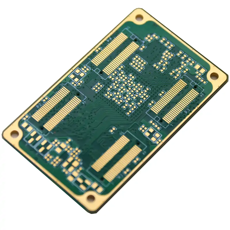
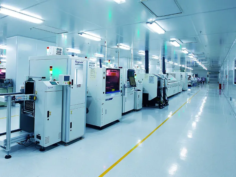 PCB ManufacturingHRPCBA is a leading PCB board manufacturer offering precision PCB fabrication services. Get high-quality boards with fast turnaround and competitive pricing
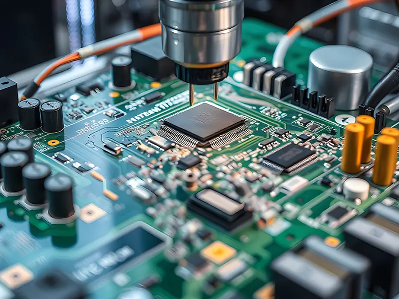 CapabilitiesDiscover HRPCBA’s robust PCB capabilities in custom PCB manufacturing services, where we transform your ideas into high-quality, functional circuit boards.