What Makes Our PCB Printer the Perfect Choice?
First, let's understand what a PCB printer is and how it's used.
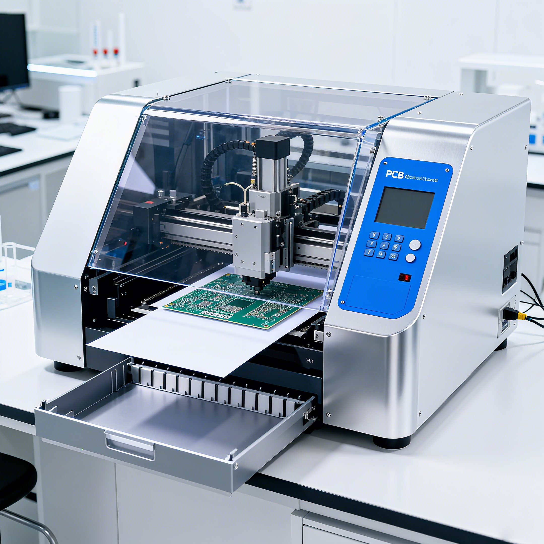
A PCB printer is a mechanical device that quickly creates PCB on a work surface. It's like a "desktop PCB factory," capable of "printing" physical circuit boards directly from computer designs.
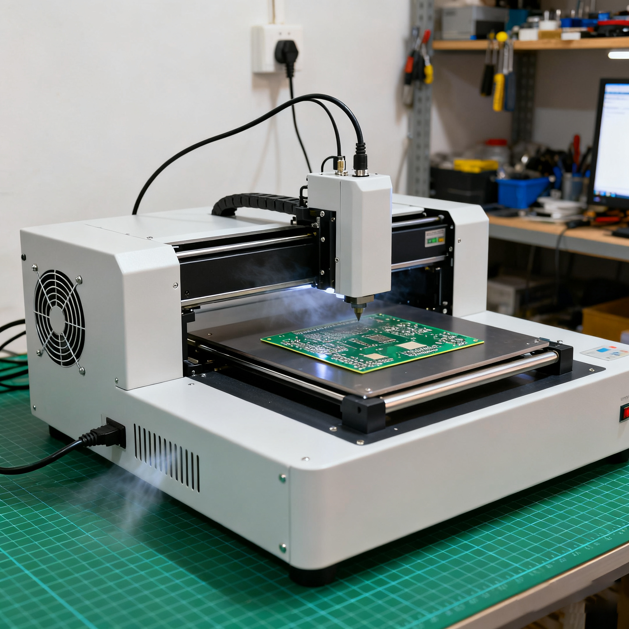
PCB printers create printed circuit boards (PCBs) by depositing conductive ink in a circuit pattern onto a substrate such as plastic or fiberglass. Rather than using traditional etching techniques, they build the circuit layer by layer, enabling rapid prototyping and home production. Advanced models can also drill holes, dispense solder paste, and reflow components, providing an all-in-one solution for manufacturing functional electronic products.
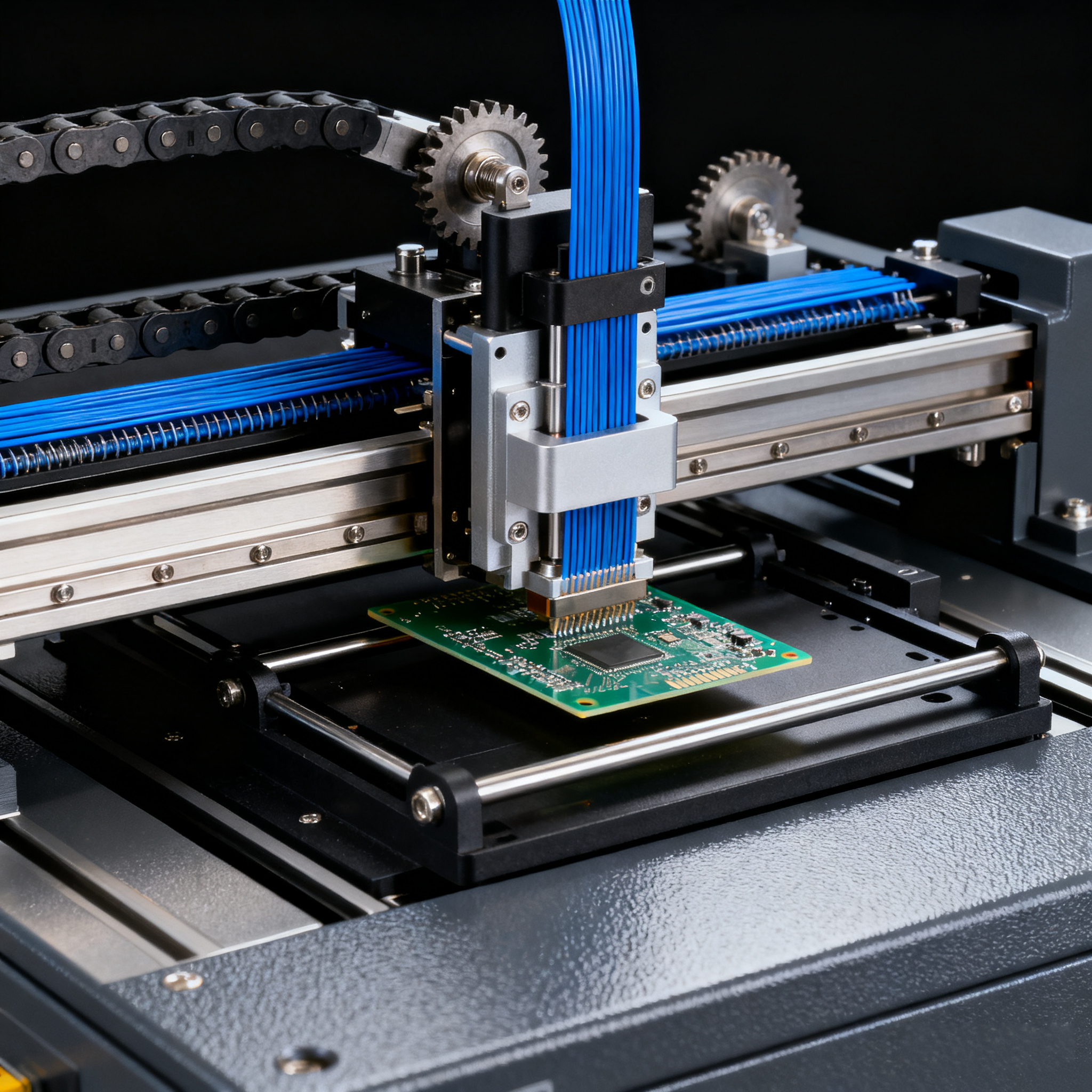
How it works
- Design: An electrical computer-aided design (ECAD) file (usually in the form of a Gerber file) is used to design the circuit.
- Substrate: Fix the substrate to the print bed. The substrate can be a rigid board (such as FR4) or a flexible board.
- Layering: A PCB printer deposits a thin layer of conductive ink (such as copper or silver) onto the substrate following the pattern on the design file.
- Curing: The deposited layers are typically cured by heating to solidify the conductive traces.
- Multilayering: This process is repeated to build a multilayer board, adding insulating layers between each conductive layer.
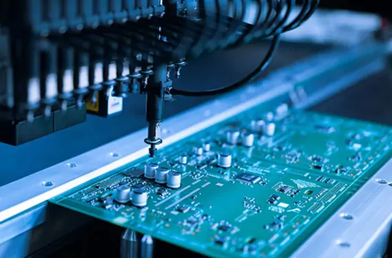
- Finishing: Some printers can also perform additional steps, such as drilling holes, applying solder paste, and reflowing components to mount them on the board.
PCB printers are currently divided into two types, one is a conductive inkjet printer, and the other is an engraving/etching integrated printer.
1. Main Type: Conductive Inkjet Printer
This is currently the most common form of "PCB printer."
- Working principle: A conductive ink printer precisely deposits metallic nanoparticle ink onto a substrate through a printhead, which then sinters to form a conductive circuit.
- Working process:
- Prepare the substrate: Place an insulating substrate (such as FR4, ceramic board, or flexible board) into the printer.
- Print the circuit: The printer reads the Gerber file and then sprays the conductive ink onto the substrate to form lines, pads and vias.
- Curing: After printing is complete, the solvent in the ink is evaporated through heating (sintering), leaving behind a solidified conductive path.
- Additive Manufacturing: Only the required material is deposited, resulting in virtually no waste and an environmentally friendly environment.
- Rapid Prototyping: From design to printed circuit board in just a few minutes.
- Design Flexibility: Designs can be easily modified and reprinted.
2. Another Type: Integrated Engraving/Etching Printer
This PCB printer "prints" circuits directly onto the copper-clad board by spraying an etchant, skipping the photolithography masking step in the traditional process.
- Working Principle: It combines mechanical engraving and chemical etching.
- Working Process:
- Coating with Resist: A layer of etching-resistant material is applied to the copper-clad board.
- Engraving: A precision milling cutter is used to scrape away the unneeded portions of the resist, exposing the copper underneath.
- Etching: The board is placed in a small etching tank within the machine. Chemical solutions only etch away the exposed copper, while the copper protected by the resist forms the circuit.
- Cleaning: Finally, the remaining resist is removed.
- Advanced technology: Adopting the concept of subtractive manufacturing, the graphics are constructed by selectively removing materials.
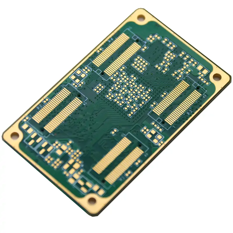
- Excellent Performance: The resulting boards are comparable to industrially produced PCBs, but with improved performance and reliability.
Why are PCB printers the ideal choice?
Key Reasons:
1. Unparalleled Speed and Convenience ("A Factory on Your Desktop")
- Instant Printing, Rapid Verification: From electronic file to physical PCB, it takes only minutes to hours. Designers can print and test immediately after completing their designs, significantly accelerating design iterations and debugging cycles, achieving "design today, verify today."
- Simplified process: It simplifies the PCB manufacturing process, skipping the traditional outsourcing steps (such as sending Gerber and BOM files to suppliers, quoting, scheduling production, shipping, etc.), shortening the waiting time from several days or even weeks to "instant waiting", significantly improving your company's R&D efficiency.
2. Extremely Low Prototyping Barrier and Cost
- No Prototyping Fees: For single-sided or simple double-sided boards, there's no need to pay factory proofing fees.
- No Minimum Order: Even a single board can be economically viable, making it ideal for verification or revisions on individual projects.
3. Unparalleled Confidentiality and Security
- In-House Completion: All sensitive design data is processed internally, eliminating the need to send design files to external manufacturers over the internet or through personnel. This fundamentally eliminates the risk of core technology leakage. This is crucial for the development of military, aerospace, or cutting-edge commercial products.
4. Strong Design Freedom and Educational Value
- Fast Iteration: Engineers and students can experiment wildly without fear of failure, as the cost of revising designs and reprinting is extremely low, greatly encouraging innovation.
- Intuitive Teaching: In education, it allows students to visually witness the creation of a circuit from virtual to physical, creating a profound learning experience.
PCB printers have a very focused and well-defined application area, primarily serving front-end applications that require extremely high speed, confidentiality, and flexibility, but less demanding performance and high-volume costs. They serve as a catalyst for innovation and accelerate R&D. They are suitable for electronics R&D and prototyping, education and training (esports competitions, etc.), scientific research projects, repair, and reverse engineering.
For a clearer understanding, we can compare PCB printers with traditional PCB manufacturing methods:
|
Application Scenarios
|
PCB Printer (Ideal)
|
Traditional PCB Factory (Preferred)
|
|
R&D stage
|
Rapid prototyping and functional verification
|
Slow speed, not suitable for rapid iteration
|
|
Education/Maker
|
Just-in-time production, manageable costs
|
Complex process, minimum spending
|
|
Confidential project
|
Complete internally, prevent leaks
|
Requires external documentation, risk of leaks
|
|
Final product
|
Suitable only for very small batch customization
|
Large-scale, high-quality, low-cost production
|
|
Circuit performance
|
Average (limited line width, accuracy, and high-frequency performance)
|
Excellent (meets industrial standards)
|
Technical Advantages:
- Modern PCB printers (primarily conductive inkjet printers) also offer the following technical features:
- Additive Manufacturing, Green and Environmentally Friendly: Compared to traditional subtractive etching methods, these printers deposit only the required material (conductive ink), producing virtually no chemical waste and being more environmentally friendly.
- Direct Printing on Shaped Surfaces: Theoretically, circuits can be printed on certain non-planar surfaces, opening up possibilities for flexible electronics or 3D integrated circuits.
- Integration: Some high-end models can simultaneously print conductive traces, insulating layers, and even solder masks and components, completing circuit board production in a single step.
Objectively Viewing Their Limitations (When They're Not "Ideal"):
To fully understand their limitations, it's important to recognize their limitations:
- Precision and Line Width Limitations: Currently, most printers cannot achieve the micron-level precision of professional PCB fabricators, making them unsuitable for boards with ultra-high IC density or extremely fine line widths.
- Inadequate Electrical Performance: The conductivity and adhesion of inks are inferior to those of traditional pure copper circuits, and through-hole metallization technology is currently immature. This makes them unsuitable for high-frequency circuits, high-current products, and applications requiring stringent long-term reliability.
- Material Cost and Complexity: Specialized conductive inks are expensive, and due to process limitations, they can typically only be produced on single- or double-layer boards, limiting the complexity of circuit designs.
- Production Efficiency: The point-by-point printing process is much slower than the large-scale batch manufacturing of traditional PCBs, making it unsuitable for mass production.
Conclusion
PCB printers excel in "speed" and "control," making them the ideal tool for rapid prototyping and in-house R&D. They dramatically shorten the time from idea to physical reality while ensuring design security, profoundly transforming electronics innovation.
When you're ready to go to market, HongRong (Shenzhen) Electronics Co., Ltd. stands as your reliable partner. With over 20 years of expertise in PCB manufacturing and assembly, we ensure your creations move seamlessly from prototype to mass production.


 PCB AssemblyHRPCBA is a PCBA China manufacturer offering high-quality PCB assembly services with full-process support, from design to assembly and testing.
 PCB ManufacturingHRPCBA is a leading PCB board manufacturer offering precision PCB fabrication services. Get high-quality boards with fast turnaround and competitive pricing
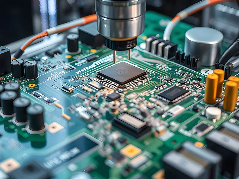 CapabilitiesDiscover HRPCBA’s robust PCB capabilities in custom PCB manufacturing services, where we transform your ideas into high-quality, functional circuit boards.