How to Change PCB Board Size in Ultiboard?
First, let's understand what Ultiboard is.
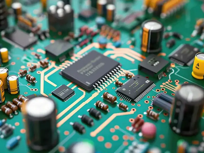
Ultiboard is a professional PCB design and layout software developed by National Instruments (NI). It provides a complete solution from schematic drawing to circuit board layout and routing.
You can think of it as software similar to Altium Designer, KiCad, or Eagle, but its core feature is its seamless integration with Multisim, which accelerates PCB prototyping.
Its main functions include:
- PCB layout: Arranges and connects electronic components according to a predetermined circuit diagram to create a fully functional and stable circuit board.
- Routing: Drawing copper traces on each layer of the PCB to connect electronic components (such as resistors, capacitors, ICs, etc.), thereby forming a fully functional and stable printed circuit board (PCB).
- Layer management: Supports multi-layer PCB design, managing signal layers, power planes, and silkscreen layers.
- Design rule checking: Ensures that the design complies with electrical and physical rules (such as line width and spacing).
- 3D preview: Visualizes the 3D model of the PCB board to check component placement and mechanical conflicts.
- Gerber file output: Generates standard Gerber files for PCB fabrication to produce the board.
Let's look at how to change the size of a PCB in Ultiboard.
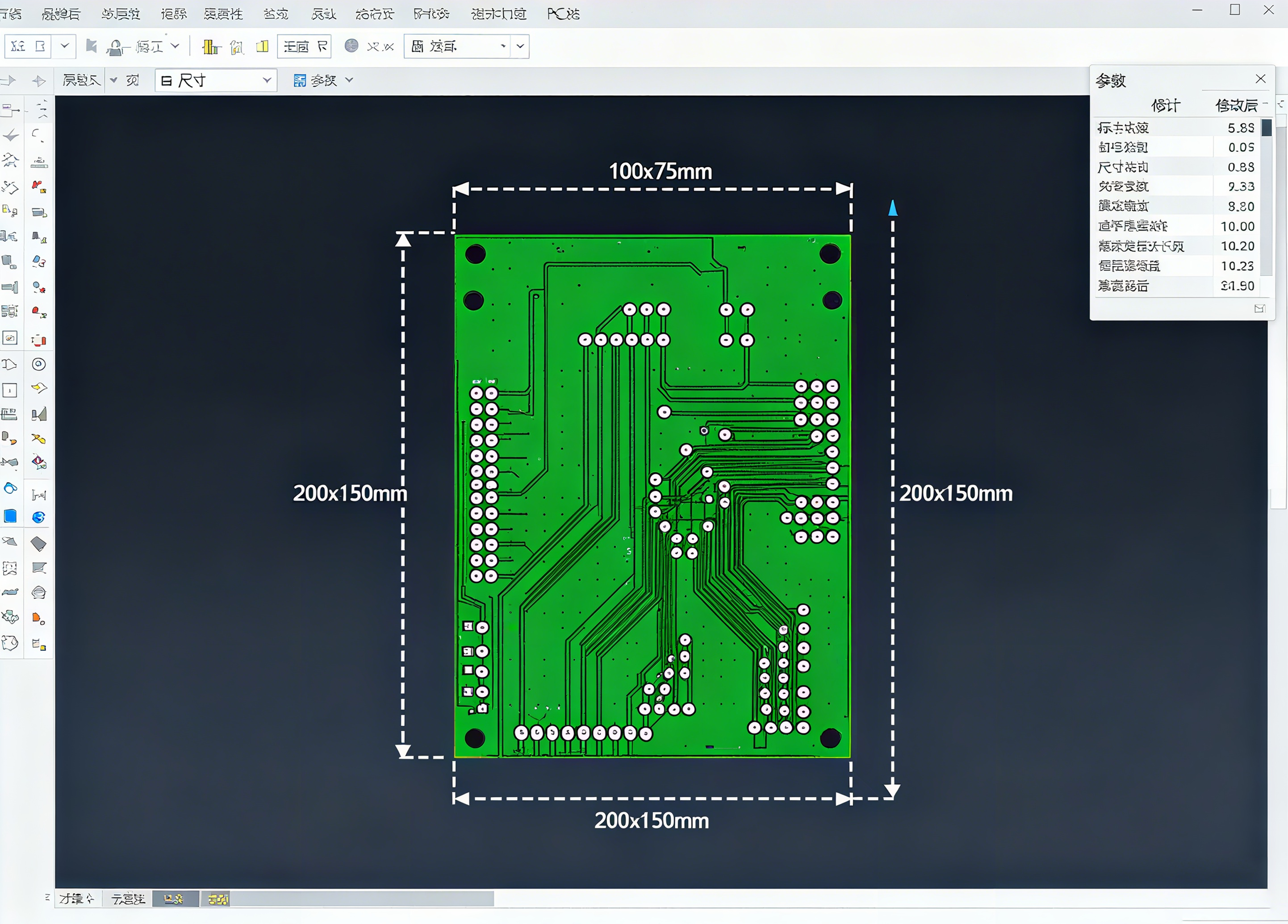
Main Method (via the "Board Outline" layer)
In Ultiboard, the size and shape of a board are defined by a dedicated "Board Outline layer." You can think of the board outline as a "cutting template" that determines the final shape of the board.Modifying the board size essentially involves adjusting the shape of this Board Outline layer. The process is very simple and consists of two main steps:
- Selecting the Correct Layer:
In the Layers panel in the lower-right corner of the window, make sure the Board Outline layer is set as the active layer. This is crucial; otherwise, you won't be able to select or modify the board outline.
- Selecting an Existing Board Outline:
Using your mouse, click on the edge of the board outline to select it. Once selected, the outline will highlight (usually becoming a dashed line or with control points).
- Editing the Shape:
- Method A: Dragging Control Points
- Once the board outline is selected, you'll see several small squares (control points) appear along the border.
- Click and drag these control points with the left mouse button to directly change the size and shape of the board outline. This method is suitable for fine-tuning or simple rectangular boards.
- Method B: Using the Properties Panel
- With the board outline selected, press F8 or open the Properties panel from the menu bar.
- In the Properties panel, you can find the board outline's geometric information. For a rectangular outline, you can directly modify its Start X, Start Y, and End X, End Y coordinates to precisely change its size and position.
- Method C: Redrawing Using Drawing Tools
- If you need to completely change the board shape (for example, from a rectangle to a circle or irregular shape), you can first delete the old outline.
- Then, select the desired shape tool (e.g., rectangle, polygon, circle, etc.) from the drawing toolbar on the left.
- Make sure the Board Outline layer is still active and redraw the desired board outline shape in the workspace
- .
Important Notes and Additional Tips
- Component Positioning: Increasing the board size is generally fine. However, if you reduce the board size, be sure the new outline does not overlap any already placed components, traces, or vias, as this will cause DRC (Design Rule Check) errors. Importing from a Netlist/PCB Manifest: Sometimes board outline information is synchronized from a front-end design tool (such as Multisim). In this case, modifying the board outline in Ultiboard may overwrite it when resynchronizing. It's best to determine the board outline during the schematic design phase or be careful to resolve conflicts when synchronizing.
- 3D View Verification: After changing the board dimensions, switch to the 3D view (View -> 3D Preview) to visually verify that the new board outline matches your expectations and that all components fit within the board.
- Board Outline and Keepout Areas: The board outline defines the physical boundaries of the board. If you need to reserve an area inside the board edge (for example, for V-cuts or tool holes), use the Keep-Out layer to draw an internal boundary.
Workflow Summary:
- Activate the layer -> Select the Board Outline layer in the Layers panel.
- Select the object -> Click the edge of the existing board outline.
- Modify the dimensions -> Drag a control point or enter precise coordinates in the Properties panel.
- Check -> Run a DRC check and view the 3D preview to ensure the design is correct.
When is Ultiboard needed?
Ultiboard is commonly used in the following scenarios:
- Education and academic research (primarily):
The combination of Ultiboard and Multisim is widely adopted by universities and vocational colleges worldwide for teaching electronic engineering, electrical engineering, and other related programs due to its ease of use and high level of integration. Students can complete the entire design process, from theoretical simulation to physical implementation, within a familiar software environment.
- Rapid prototyping and verification:
When engineers come up with a good idea, they typically first simulate and test the circuit in Multisim. Once they've confirmed its feasibility, they can now transfer the design directly to Ultiboard software for physical circuit board design with a single click. This seamless process eliminates the hassle and errors associated with manual file conversion, significantly speeding up prototyping.
- Developing relatively simple electronic products:
For electronic products of less complex design (such as simple control boards, power boards, and experiment boards), Ultiboard provides sufficient functionality to complete the design task. It is well-suited for small to medium-sized projects.
In contrast, engineers may choose more advanced specialized tools (such as Altium Designer and Cadence Allegro) in the following situations:
- Designing extremely complex, high-speed digital circuits (such as high-end processors, FPGAs, and multi-channel DDR memory).
- Requirement for advanced SI/PI (signal integrity/power integrity) analysis.
- Designing high-density interconnect (HDI) boards.
- Collaborating with large teams (Ultiboard's team collaboration capabilities are not as robust as specialized software).
What type of staff is typically needed to operate Ultiboard?
Those who operate Ultiboard are typically engineers or technicians responsible for the "backend" or "implementation" phase of the electronics design process. These include:
- Electronic Engineers/Hardware Engineers:
Especially those who graduated from universities using the Multisim/Ultiboard system. These engineers typically complete the entire process, from schematics and simulation to PCB layout, independently. In small and medium-sized companies or startups, hardware engineers often need to operate PCB design tools themselves.
- PCB Layout Engineers/Technicians:
Larger companies typically have dedicated layout engineers. They receive Multisim schematics from electronics engineers and then perform physical layout, routing optimization, DRC checks, and production file output in Ultiboard. Therefore, they must be very familiar with DFM (Design for Manufacturability) and DFA (Design for Assembly) rules.
- Teachers and Students:
This is Ultiboard's largest user group. Teachers use it for teaching, while students use it for course projects, graduation projects, or e-sports competitions, learning the complete electronic product design process.
Required Skills:
- Electronic circuit fundamentals: Understand circuit principles and be able to interpret schematics.
- Familiarity with PCB manufacturing processes: Understanding process requirements such as line width, line spacing, vias, and solder mask.
- Proficiency in Ultiboard operation: Familiarity with Ultiboard features such as layer management, routing techniques, batch operations, and 3D viewing.
- Care and Patience: PCB design requires extreme care and patience; even the smallest mistake can render an entire batch of boards scrapped.
Changing PCB dimensions in Ultiboard is often done for the following key reasons:
1. Optimizing space and reducing costs (the most common reason)
- Reducing board size: After completing layout and routing, a large amount of blank space is discovered on the board. To save costs (PCB price is often directly related to size), the board frame needs to be reduced to remove excess space.
- Adapting to an enclosure: The mechanical engineer provides the final 3D model of the enclosure, and the PCB must be reduced to fit within the mounting space and mounting posts.
2. Optimize the board for existing requirements
- Adding new circuitry: If new features or interfaces need to be added later in the project, the existing space may be insufficient, necessitating an expansion of the board to accommodate the new components and circuitry.
- Improve component layout: If the initial layout is too crowded, routing can become difficult or heat dissipation can be poor. Increasing the board size provides more room for components to operate, improving performance and reliability.
- Adding mounting holes: If the required mounting holes extend beyond the current board edge, the board's outer dimensions must be expanded accordingly.
3. Correcting initial design errors
- At the beginning of a project, engineers often estimate board dimensions based on experience. However, after placing all components, they may discover that the initial board dimensions were incorrectly estimated, either too large or too small. This is when adjustments are necessary.
4. Adapting to specific manufacturing specifications
- Meeting board fabrication capabilities: PCB fabricators may have specific requirements for maximum or minimum board dimensions. For example, certain low-cost prototyping processes may limit the maximum dimensions, requiring design adjustments accordingly.
- Paneling requirements: For ease of production and assembly, multiple small boards need to be assembled into a large board (panelization). In this case, the size or shape of the individual boards may need to be slightly adjusted to ensure the most compact and economical arrangement on the panel.
5. Changing the board shape
- Non-rectangular design: Engineers often initially design a board into a simple rectangle, but to accommodate project requirements (curved or other irregular shapes), they need to modify the rectangular board frame into a custom shape (such as a circle, a rectangle with grooves, etc.).
About other questions
- How to alter trace width in Ultiboard?
Within Ultiboard, you may preset default line widths via ‘Design Rules’ prior to routing to ensure compliance with design specifications. During routing, pressing the “Tab” key allows real-time modification of the current trace width. For completed traces, right-click and select ‘Properties’ to subsequently adjust their width.
- How to change PCB dimensions in Altium?
To change PCB dimensions in Altium Designer, simply redefine the board shape by navigating to Design > Board Shape > Redefine Board Shape, then trace the new outline in the workspace. This action updates the physical PCB size and can also be done by modifying the board outline in a mechanical layer.


 PCB AssemblyHRPCBA is a PCBA China manufacturer offering high-quality PCB assembly services with full-process support, from design to assembly and testing.
 PCB ManufacturingHRPCBA is a leading PCB board manufacturer offering precision PCB fabrication services. Get high-quality boards with fast turnaround and competitive pricing
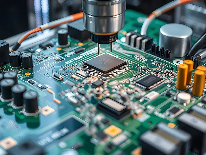 CapabilitiesDiscover HRPCBA’s robust PCB capabilities in custom PCB manufacturing services, where we transform your ideas into high-quality, functional circuit boards.