Electronics are getting smaller, yet they demand more power and speed. Smartphones, IoT devices, and high-performance computing systems rely on compact circuit boards packed with advanced technology. This shift has pushed high-density PCB innovation forward, enabling manufacturers to build thinner, faster, and more efficient boards.
High-Density Interconnect (HDI) PCBs make this possible. They use advanced materials, fine-pitch assembly, and microvia technology to increase component density without sacrificing performance. As industries push for even more powerful devices in smaller footprints, PCB manufacturing must evolve. This article dives into the innovations making it happen.
Microvia Technology: The Backbone of HDI PCBs
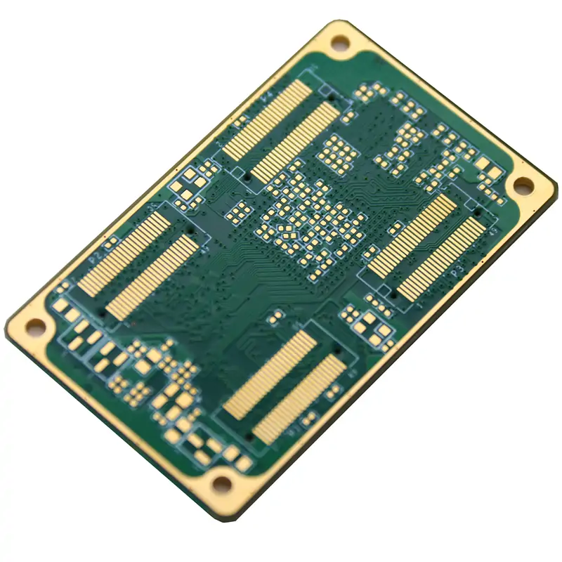
Microvias are at the heart of high-density PCB innovation. These tiny holes connect different board layers, making it possible to stack multiple circuits while keeping the board size minimal. Unlike traditional through-hole vias, microvias don’t go through the entire PCB. They connect only the necessary layers, allowing for denser layouts and more efficient signal routing.
HDI PCBs use different types of microvias depending on design needs. Blind microvias link outer layers to internal ones without breaking through the entire board, helping maximize surface space for components. Buried microvias connect internal layers, keeping the outer surfaces free for high-density placement. Some designs use stacked microvias for a direct vertical connection, while others opt for staggered microvias to improve thermal management and signal integrity.
This technology allows manufacturers to shrink device sizes without losing performance. Microvias reduce electrical resistance, minimize signal loss, and improve reliability compared to traditional vias. That’s why they’re essential in advanced PCBs used in everything from smartphones to medical devices.
Fine-Pitch Assembly: Packing More Power in Less Space
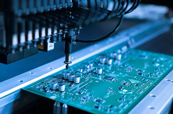
Smaller components demand higher precision. Fine-pitch assembly makes this possible by placing components closer together, increasing board density without adding bulk. Traditional PCB assembly methods struggle with these ultra-small connections, but modern advanced PCBA techniques ensure accuracy and reliability.
The biggest challenge is soldering precision. As component sizes shrink, tiny solder pads must align perfectly. Even the slightest miscalculation can cause defects. Solder bridging, where excess solder forms unintended connections, is a common issue. So is tombstoning, where one side of a component lifts off the board during soldering, rendering it useless.
To solve these problems, manufacturers rely on Surface Mount Technology (SMT). Automated pick-and-place machines position components with microscopic accuracy, ensuring a flawless assembly. Reflow soldering techniques carefully control heat to prevent defects. These innovations have made fine-pitch assembly the industry standard for high-performance, compact PCBs.
For a closer look at how fine-pitch components are assembled, check out this SMT assembly guide.
Fine-pitch assembly is a critical part of high-density PCB innovation. It allows manufacturers to build complex circuits into ultra-compact spaces, pushing the boundaries of what modern electronics can achieve.
Advanced Materials for Higher Durability and Performance
Not all circuit boards are built the same. Traditional PCBs use materials that work fine for basic electronics, but high-density PCB innovation demands something more advanced. With thinner traces, stacked layers, and micro-sized components, HDI PCBs need materials that can handle extreme conditions without failing.
One of the biggest concerns is heat. High-speed electronics generate more heat than ever, and standard PCB materials struggle to keep up. That’s why manufacturers are switching to high-Tg laminates, which offer better heat resistance and prevent warping. Another game-changer is low-loss substrates, which reduce signal interference in high-frequency applications like 5G and AI-driven systems.
Flexible materials are also on the rise. With the explosion of wearables and compact consumer devices, PCBs must bend and flex without breaking. New material innovations make it possible to create ultra-thin, flexible circuit boards that fit into curved surfaces without sacrificing performance. These advances allow designers to push the limits of what’s possible in modern electronics.
Flexible materials are also on the rise. With the explosion of wearables and compact consumer devices, PCBs must bend and flex without breaking. New material innovations make it possible to create ultra-thin, flexible circuit boards that fit into curved surfaces without sacrificing performance. These advances allow designers to push the limits of what’s possible in modern electronics.
Laser Drilling: Enabling Ultra-Precision PCB Manufacturing
As PCBs shrink, traditional manufacturing techniques just can’t keep up. Mechanical drilling works fine for standard circuit boards, but it struggles with microvias and fine-pitch layouts. That’s where laser drilling comes in.
Laser drilling uses high-precision beams to create tiny, clean holes for microvias. Unlike mechanical drills, which wear out over time, lasers produce consistent and accurate results on every board. This precision is critical for high-density PCB innovation, where even the slightest misalignment can cause failures.
Another major advantage is reduced material stress. Mechanical drilling applies pressure that can crack or weaken the board, especially on thin, multi-layer designs. Laser drilling eliminates this risk, ensuring durability even in ultra-compact circuits.
The process is also faster. With automated laser systems, manufacturers can drill thousands of microvias in minutes, speeding up production without compromising quality. This innovation has become a must-have for modern advanced PCBA techniques, helping create smaller, more powerful devices with greater reliability.
The Rise of 5G and AI: How They Push HDI PCB Limits
Next-gen technologies demand next-gen circuit boards. The rollout of 5G networks and the rise of AI-driven hardware have pushed high-density PCB innovation to new heights. These technologies require PCBs that can handle higher speeds, lower latency, and extreme processing power—all while staying compact.
5G devices need ultra-fast signal transmission. Standard PCBs struggle with this because traditional materials and layouts cause signal loss at high frequencies. That’s why HDI PCBs now use advanced low-loss substrates and optimized trace designs to maintain signal integrity. Without these improvements, 5G performance would suffer.
AI hardware presents a different challenge. Machine learning models and AI chips process massive amounts of data in real time, generating heat and requiring more layers, faster connections, and compact footprints. HDI PCBs make this possible by integrating fine-pitch components, high-speed signal pathways, and advanced cooling solutions.
As 5G and AI continue to evolve, advanced PCBA techniques will need to keep up. The demand for ultra-high-density, high-performance circuit boards will only grow, pushing the boundaries of what HDI PCBs can achieve.
Automation and AI in HDI PCB Manufacturing
Building high-density PCBs is no longer just about precision—it’s about speed and efficiency. As circuit designs become more complex, manufacturers are turning to automation and AI to improve accuracy, reduce waste, and streamline production.
AI-driven design tools are making a huge impact. Engineers no longer have to manually fine-tune every trace and via placement. Instead, AI algorithms optimize PCB layouts for maximum efficiency, reducing signal interference and improving performance. These tools can simulate how a PCB will function before it's even built, catching potential issues early and cutting down on costly redesigns.
On the factory floor, automated optical inspection (AOI) ensures defect-free production. Instead of relying on human inspectors, AI-powered machines scan finished boards at high speed, detecting even the smallest flaws in soldering, component placement, or via alignment. This not only improves quality control but also increases production speed.
Robotics also play a key role in advanced PCBA techniques. Automated pick-and-place machines can handle ultra-fine-pitch components with extreme precision, ensuring each part is placed perfectly on the board. Combined with laser drilling and AI-driven design, automation is pushing PCB manufacturing into the future.
Future Trends: Where HDI PCB Innovation is Headed
The demand for smaller, faster, and more powerful circuit boards isn’t slowing down. In fact, innovation is accelerating, bringing new possibilities to PCB manufacturing.
One of the most exciting developments is 3D-printed PCBs. While traditional manufacturing builds circuit boards layer by layer, 3D printing could revolutionize the process by allowing fully custom, highly compact designs in a fraction of the time. This technology is still in its early stages, but the potential is enormous.
Sustainability is another major focus. As electronics production grows, so does e-waste. Manufacturers are now looking for eco-friendly materials that reduce environmental impact without sacrificing performance. Biodegradable PCB substrates and lead-free soldering processes are already becoming industry standards.
Wearable technology, AR/VR devices, and next-gen IoT applications will continue pushing high-density PCB innovation forward. Flexible PCBs, ultra-thin substrates, and even self-healing circuits are on the horizon. The future of HDI PCB manufacturing is all about adapting to new challenges while maintaining precision, reliability, and efficiency.
Conclusion: Why HDI PCBs Are the Future of Electronics
High-Density Interconnect PCBs are shaping the future of modern electronics. From microvias and fine-pitch assembly to laser drilling and AI-driven automation, innovation is driving PCB manufacturing forward at an incredible pace. These advancements allow for smaller, faster, and more reliable devices, meeting the ever-growing demand for high-performance technology.
As industries push for more compact and powerful hardware, manufacturers must adopt advanced PCBA techniques to stay competitive. Whether it's 5G, AI, IoT, or next-gen computing, HDI PCBs are at the core of today’s most groundbreaking innovations.
To explore how high-density PCB innovation can enhance your projects, check out cutting-edge HDI PCB manufacturing and stay ahead of the curve.


 PCB AssemblyHRPCBA is a PCBA China manufacturer offering high-quality PCB assembly services with full-process support, from design to assembly and testing.
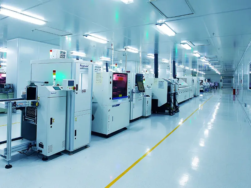 PCB ManufacturingHRPCBA is a leading PCB board manufacturer offering precision PCB fabrication services. Get high-quality boards with fast turnaround and competitive pricing
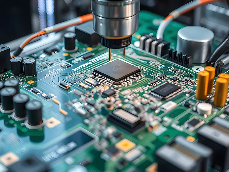 CapabilitiesDiscover HRPCBA’s robust PCB capabilities in custom PCB manufacturing services, where we transform your ideas into high-quality, functional circuit boards.