HRPCBA is a leading PCB board manufacturer offering precision PCB fabrication services. Get high-quality boards with fast turnaround and competitive pricing
Discover HRPCBA’s robust PCB capabilities in custom PCB manufacturing services, where we transform your ideas into high-quality, functional circuit boards.
What Is an HDI PCB and Why Is It So Important in Modern Electronics?
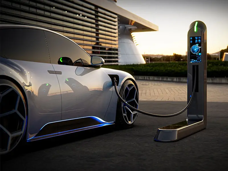
Over the past decade, electronic devices have become thinner, lighter, smarter, and more powerful than ever before. From 5G smartphones and AI servers to electric vehicles and wearable devices, one critical technology powers this evolution behind the scenes: the HDI PCB (High Density Interconnect Printed Circuit Board).
If you previously read our article “How Does HongRong’s PCB Solder Mask Protect Your Board?”, you already understand how solder mask technology improves PCB reliability. Today, we will go deeper into the world of HDI PCB technology and explain why it has become the foundation of modern electronic design.
1. What Is an HDI PCB?
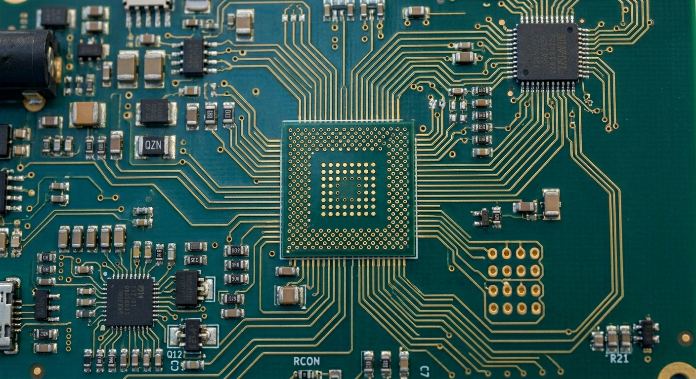
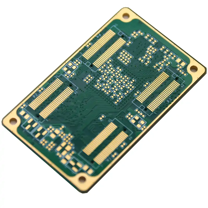
HDI (High Density Interconnect) refers to an advanced PCB technology with significantly higher wiring density than conventional printed circuit boards. According to the IPC-2226 standard, HDI PCBs achieve greater circuit integration within limited board space by using finer traces, smaller vias, and more complex interconnection structures.
Simply put, if a traditional PCB is like a standard city road system, an HDI PCB is more like a modern smart city with underground tunnels, elevated highways, and multi-level transportation networks.
Key Features of HDI PCB:
Microvias, Blind Vias & Buried Vias
Fine Trace Width and Spacing
High-Density Component Placement
Multi-Level HDI Structures
Any-Layer Interconnection Technology
1) Microvias and Buried Via Technology HDI PCBs typically use laser-drilled microvias and buried vias with diameters smaller than 0.15mm. This design significantly shortens signal transmission paths and improves routing efficiency.
2) Ultra-Fine Circuit Design HDI boards can achieve trace width and spacing as small as 0.10mm (4mil) or even smaller, allowing far more circuit connections within limited PCB space.
3) Multi-Level HDI Structures Current mainstream HDI stack-up structures include:
HDI Structure
Features
1+N+1
Entry-level HDI design
2+N+2
Higher routing density
3+N+3
Advanced complex applications
Any-Layer HDI
Maximum routing flexibility
2. Why Is HDI PCB So Important?
As electronic products continue evolving toward miniaturization, higher performance, and faster signal transmission, conventional PCBs are increasingly unable to meet modern design requirements.
The importance of HDI PCB technology can be seen in several key areas: 1) Enabling Smaller and Thinner Electronics
HDI technology allows engineers to integrate more functionality into much smaller PCB footprints.Modern smartphones, wireless earbuds, and smartwatches achieve compact sizes while maintaining powerful performance largely because of HDI PCB technology.
2) Improving Signal Integrity
HDI PCBs use shorter signal paths and smaller vias, which helps reduce:
Signal Loss
Impedance Mismatch
EMI
Signal Reflection
This is especially critical for 5G communications, AI computing, high-speed servers, and data networking systems.
3) Enhancing Reliability Because microvias have lower aspect ratios, HDI PCBs generally provide better long-term reliability under thermal cycling, vibration, and harsh operating conditions than conventional through-hole PCBs.For this reason, HDI technology is widely used in automotive electronics, industrial controls, and medical devices.
4) Supporting Rapidly Growing Market Demand Driven by rapid growth in 5G, AI, electric vehicles, and IoT devices, the global HDI PCB market continues expanding rapidly.
Global HDI PCB Market Trends:
Category
Data
China HDI Market Size (2024)
RMB 45.568 Billion
Global HDI Market (2025)
USD 17.78 Billion
Global HDI Market (2026)
USD 19.47 Billion
Forecast Market Size (2030)
USD 28.82 Billion
3. Main Applications of HDI PCB Today, HDI PCB technology is used across nearly every advanced electronics sector.
Industry
Typical Applications
Consumer Electronics
Smartphones, Tablets, Wearables
Automotive Electronics
ADAS, Radar, Infotainment Systems
Medical Devices
Pacemakers, Monitors, Ultrasound Systems
Telecommunications
5G Base Stations, Network Switches
AI & Servers
AI Accelerators, High-Performance Servers
IoT Devices
Smart Home Devices, Industrial Sensors
4. Why Choose HongRong as Your HDI PCB Partner? HDI PCB manufacturing requires not only advanced engineering design but also extremely precise manufacturing and quality control capabilities.
Founded in 1998, HongRong (Shenzhen) Electronics Co., Ltd. has specialized in PCB manufacturing and PCBA assembly services for over two decades, with extensive experience in HDI and complex multilayer PCB solutions. HongRong’s Core Advantages:
25+ Years of Industry Experience
One-Stop PCB & PCBA Solutions
ISO/IATF/UL Certified
Fast Prototyping & Delivery
Customers in 30+ Countries
Professional Engineering Support
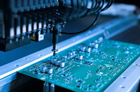
We provide complete turnkey solutions covering PCB design optimization, component sourcing, HDI PCB fabrication, and PCBA assembly testing, supporting everything from rapid prototyping to mass production.Supported by Shenzhen’s mature electronics supply chain ecosystem, we offer 2-hour quotations, 48-hour prototype delivery, and reliable large-scale production capabilities.
5. Conclusion
HDI PCB is no longer just an advanced PCB technology—it has become a core foundation driving innovation across the modern electronics industry.
From smartphones and AI servers to electric vehicles and medical devices, HDI technology continues pushing electronics toward smaller size, faster speed, and greater performance. If you are looking for a reliable HDI PCB and PCBA manufacturing partner, HongRong’s engineering team is ready to support your next project.


 PCB AssemblyHRPCBA is a PCBA China manufacturer offering high-quality PCB assembly services with full-process support, from design to assembly and testing.
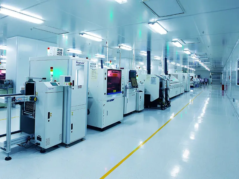 PCB ManufacturingHRPCBA is a leading PCB board manufacturer offering precision PCB fabrication services. Get high-quality boards with fast turnaround and competitive pricing
 CapabilitiesDiscover HRPCBA’s robust PCB capabilities in custom PCB manufacturing services, where we transform your ideas into high-quality, functional circuit boards.