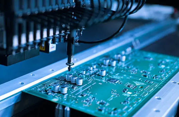
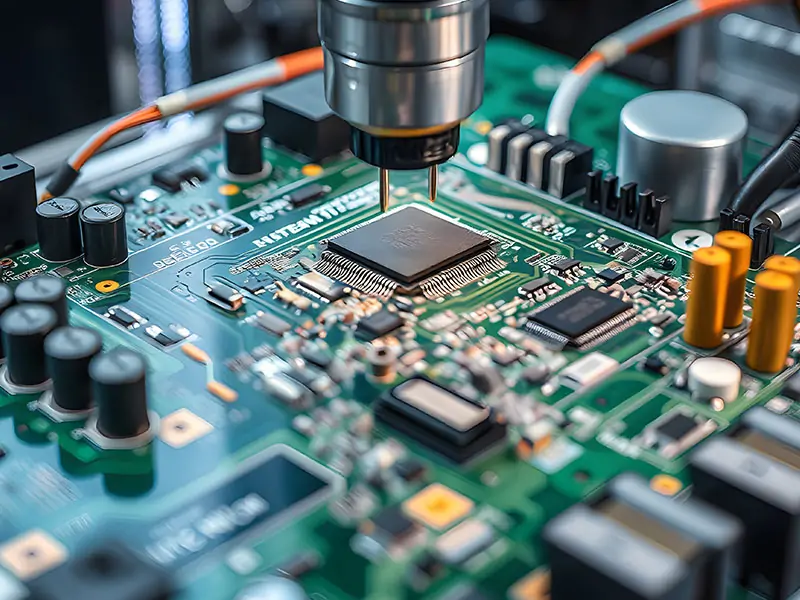
When you open a smartphone, computer, automotive electronic system, or even a common home appliance, you will usually find one or more circuit boards inside. Chips, resistors, capacitors, connectors, and other electronic components are mounted on these boards. They are not connected randomly. Instead, they are connected through a carefully designed PCB (Printed Circuit Board).
A PCB may look like a simple flat board, but it performs an important job inside an electronic product. It provides a place to mount components and creates organized electrical paths for power and signals.
So, what exactly is a PCB? How does it work? And why is it so important to modern electronics?
This guide explains the basics from a practical point of view, without assuming that you already have an engineering background.
What Is a PCB?
PCB stands for Printed Circuit Board.
In simple terms, a PCB is a manufactured platform used to support and electrically connect electronic components. Conductive copper structures are formed on or inside the board according to the circuit design.
Think about an electronic product as a complete system. Different components perform different functions, while the PCB provides the physical and electrical connections that allow those components to work together.
For example, a simple LED circuit may contain a power source, a resistor, and an LED. Copper traces on the PCB connect these parts so that current can follow the intended electrical path.
That is why a PCB is not an electronic component by itself. It is better understood as the foundation of an electronic circuit.
For someone new to electronics, the simplest way to remember it is:
A PCB is the platform used to mount and connect electronic components.
What Is a PCB Made Of?
PCB construction varies depending on the application, but a typical PCB contains several basic elements.
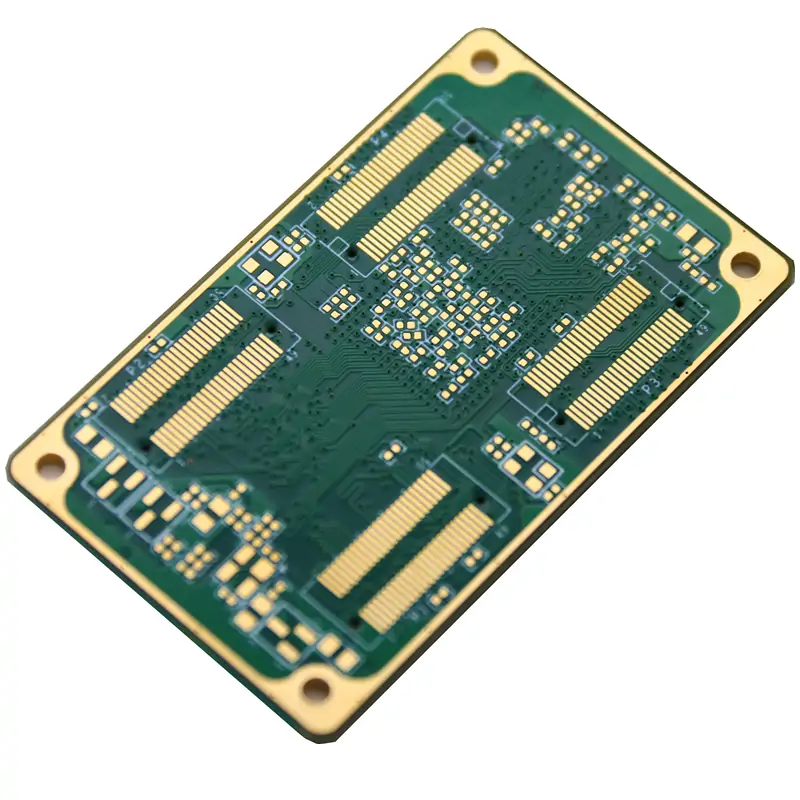
The substrate forms the base of the board. It provides mechanical support and electrical insulation. FR-4 is one of the commonly used material systems for rigid PCBs, although different applications may require different materials.
The copper layers provide the main conductive structures. After the PCB is manufactured, parts of these copper layers form traces, pads, power areas, and ground areas.
Pads are the connection points where electronic components are soldered to the PCB.
Vias are plated holes that allow electrical connections to pass between different conductive layers. They become particularly important when a PCB has multiple layers.
You may also notice a colored coating covering much of the board. This is the solder mask. Green is a common solder mask color, but PCBs can be produced in other colors as well. The solder mask protects selected copper areas and helps prevent unwanted solder connections. For more detail, see How Does HongRong’s PCB Solder Mask Protect Your Board?.
The printed letters and symbols on a PCB are generally part of the silkscreen. Markings such as R1, C2, and U1 help identify components and their locations during assembly, testing, and maintenance.
Together, these elements form the PCB that we see in an electronic product.
How Does a PCB Actually Work?
One of the easiest ways to understand a PCB is to look at the development process behind it.
A typical electronic project may follow a path like this:
Schematic → PCB Layout → PCB Fabrication → Component Assembly → Testing
The schematic describes the electrical relationships between components. It tells the designer which components need to be connected.
The PCB layout takes those electrical relationships and turns them into a physical design. It determines where components are placed and how the conductive paths are routed.
Designers also need to consider questions such as:
-
Where should each component be placed?
-
How should power and ground be distributed?
-
How should signals be routed?
-
Where should different PCB layers be connected?
-
What board size and mounting features are required?
Once the design is completed, manufacturing data is used to fabricate the PCB.
If components also need to be installed, the project moves into PCB assembly, creating a PCBA.
So, the important part of a PCB is not simply that it contains many lines. Those lines and structures are designed to perform specific electrical and mechanical functions.
For more information about the design process, you can read How to Design a PCB Board from Schematic to Layout?.
What Are the Main Types of PCBs?
There is no single PCB structure that works for every product. Board requirements change depending on circuit complexity, available space, performance requirements, and manufacturing needs.
| PCB Type |
Simple Explanation |
Common Characteristics |
| Single-Sided PCB |
One main conductive layer |
Simple structure and limited routing space |
| Double-Sided PCB |
Conductive layers on both sides |
More routing flexibility |
| Multilayer PCB |
Multiple conductive layers |
Suitable for complex and high-density circuits |
| Flexible PCB |
A PCB that can flex or bend |
Useful where space or movement is a concern |
| Rigid-Flex PCB |
Rigid and flexible sections combined |
Suitable for space-constrained designs |
| HDI PCB |
High-density interconnection structure |
Designed for compact, high-density electronics |
For example, multilayer PCBs create additional routing space by using multiple copper layers rather than simply making the board larger.
As circuits become more complicated, this approach can help engineers fit more connections into a limited area. You can learn more in How Multilayer PCB Technology Supports Advanced Electronics?.
However, more layers do not automatically mean a better PCB. The board structure should match the actual requirements of the product. Using an unnecessarily complex PCB can increase manufacturing difficulty and cost.
Why Is a PCB Essential to Modern Electronics?
The importance of a PCB becomes easier to understand when we look at what it does in a real product.
It Keeps Components Connected
Electronic products can contain a large number of components.
If every component had to be connected with separate wires, the wiring could quickly become difficult to manage. It could also make assembly, maintenance, and product design more complicated.
A PCB fixes these electrical connections into a defined structure, making the circuit easier to manufacture consistently.
It Helps Save Space
Electronic products continue to become smaller while offering more functions.
Double-sided routing, multilayer structures, and high-density PCB technologies allow more electrical connections to fit into a limited space.
This is one reason PCBs are widely used in smartphones, smart devices, communication equipment, industrial electronics, and many other compact products.
It Makes Production More Consistent
PCB layouts are created from defined design data.
After a design has been verified, the same board structure can be manufactured repeatedly according to the specified requirements. This is particularly important for products that need stable production across multiple batches.
It Can Affect Product Performance
A PCB is more than a passive support for components.
Trace routing, layer arrangement, grounding, materials, impedance, and other design factors can affect signal integrity, power distribution, and electromagnetic compatibility.
For this reason, a PCB needs to be designed and manufactured according to the actual requirements of the electronic system.
It Connects Product Design With Manufacturing
Taking an electronic product from an idea to mass production involves several stages, including design, engineering validation, PCB fabrication, component sourcing, assembly, and testing.
The PCB sits at the center of this process.
This is why choosing a PCB supplier is not only about whether a factory can produce a board. Engineering support, manufacturing capability, quality control, and assembly experience can also make a difference to the final project.
PCB vs. PCBA: What Is the Difference?
This is one of the most common points of confusion for people who are new to electronics.
A PCB is the circuit board itself, while a PCBA is a PCB with electronic components assembled onto it.
For example, a newly manufactured bare board without resistors, capacitors, ICs, or connectors installed is a PCB.
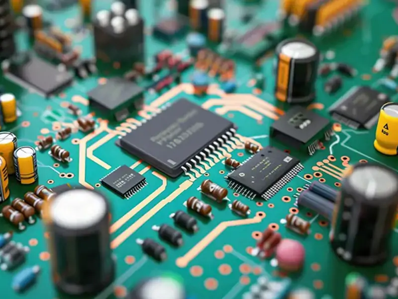
Once electronic components are mounted and soldered onto the board through processes such as SMT or through-hole assembly, it becomes a PCBA (Printed Circuit Board Assembly).
|
PCB |
PCBA |
| Meaning |
Printed Circuit Board |
Printed Circuit Board Assembly |
| Components |
Usually not assembled |
Components are assembled |
| Main Role |
Provides the electrical and mechanical foundation |
Forms a functional electronic assembly |
| Manufacturing Stage |
PCB fabrication |
Assembly and testing |
If a customer only needs bare circuit boards, PCB fabrication may be enough.
If the project requires PCB fabrication, component sourcing, SMT/THT assembly, and testing, then a PCBA service is more appropriate.
For customers, working with a supplier that can coordinate PCB fabrication and assembly can also simplify communication and project management. HRPCBA provides one-stop PCB and PCBA manufacturing services for customers with different production requirements.
What Should You Consider When Choosing a PCB?
You do not need to be a PCB design engineer to understand the basic questions that matter when selecting a PCB supplier.
Start with the product itself.
How complex is the circuit?
Circuit complexity can affect the required number of PCB layers, routing density, and board structure.
How much space is available?
A compact product may require a higher-density PCB solution.
What environment will the PCB operate in?
Temperature, humidity, mechanical stress, and the way the product is used can influence material and construction choices.
How many boards are required?
Prototype, small-batch, and mass-production projects may have different manufacturing and quality requirements.
Do you need a PCB or a complete PCBA?
This is worth confirming before requesting a quotation.
If you need a supplier to handle PCB fabrication as well as component sourcing, assembly, and testing, a one-stop PCB and PCBA supplier can make the overall production process easier to coordinate.
Conclusion
A PCB may look like a simple board, but its role inside an electronic product is much more important than its appearance suggests.
It provides a physical foundation for electronic components and creates defined paths for power and signals. As electronic products become smaller, faster, and more complex, PCB design and manufacturing requirements become increasingly demanding.
From consumer electronics and automotive systems to industrial controls, medical equipment, communication devices, and energy products, PCBs remain a fundamental part of modern electronics.
For businesses sourcing PCBs, price is only one part of the decision. Manufacturing capability, engineering support, quality control, PCBA assembly capability, and delivery management are also worth considering.
If a project requires more than a bare board, choosing a supplier that can coordinate PCB fabrication, component sourcing, SMT/THT assembly, and testing can make the production process more straightforward.
HRPCBA provides one-stop PCB manufacturing and PCBA assembly services, supporting PCB fabrication, SMT assembly, THT assembly, turnkey PCBA, and related testing services for customers with different electronic manufacturing requirements.



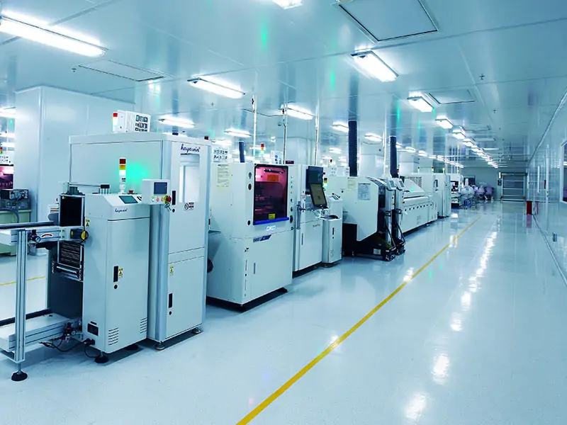
 PCB AssemblyHRPCBA is a PCBA China manufacturer offering high-quality PCB assembly services with full-process support, from design to assembly and testing.
 PCB ManufacturingHRPCBA is a leading PCB board manufacturer offering precision PCB fabrication services. Get high-quality boards with fast turnaround and competitive pricing
 CapabilitiesDiscover HRPCBA’s robust PCB capabilities in custom PCB manufacturing services, where we transform your ideas into high-quality, functional circuit boards.