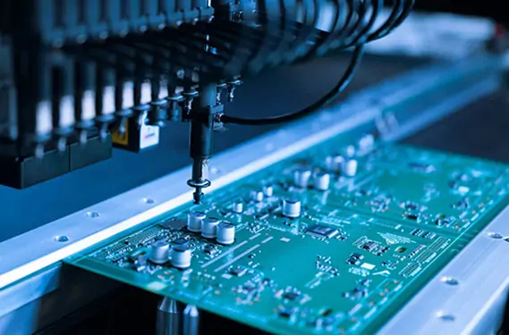
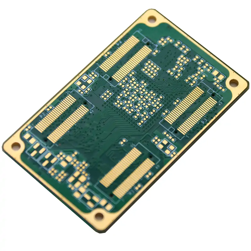
Open a modern electronic device and there is a good chance that the PCB inside is doing much more than simply connecting components. Processors, memory, sensors, communication interfaces, power circuits, and connectors may all need to work on the same board. The available space, however, is usually limited.
That creates a practical PCB design problem: where should all those connections go?
Adding more routing layers is one way to solve it. A multilayer PCB gives the designer more room to distribute signals, power, and ground connections. It can also make it easier to build a suitable electrical environment for high-speed signals.
But adding layers is not a shortcut. An eight-layer PCB is not automatically better than a four-layer PCB. The stack-up has to make sense for the circuit, and it has to be something the manufacturer can build consistently.
So, when engineers talk about multilayer PCB technology, the discussion is really about how the layers are used, not just how many layers are present.
What Is a Multilayer PCB?
A multilayer PCB contains multiple conductive copper layers separated by insulating dielectric material. These layers are pressed together during the manufacturing process to form one board.
A basic six-layer example might look like this:
| Layer |
Possible Function |
| L1 |
Components and signal routing |
| L2 |
Ground/reference plane |
| L3 |
Signal routing |
| L4 |
Power distribution |
| L5 |
Ground/reference plane |
| L6 |
Signal routing |
This is only an example. A real stack-up can look quite different depending on the circuit.
The choice of layer arrangement becomes more important as signal speeds increase. A signal trace does not work independently of the rest of the PCB. Its nearby reference plane, dielectric material, trace dimensions, and surrounding structures all influence its electrical behavior.
For this reason, stack-up planning should happen alongside PCB layout rather than being left until the manufacturing stage.
The basic construction of multilayer boards is covered in more detail in HRPCBA's multilayer PCB manufacturing information.
Why Do Advanced Electronics Use Multilayer PCBs?
The most obvious reason is routing space.
On a simple two-layer board, most connections have to share the top and bottom copper layers. Once component density increases, routing can become difficult. A BGA package is a good example. The outer connections may be relatively easy to reach, while the inner rows have to be routed through increasingly crowded areas.
With additional copper layers, those connections can be spread out.
That does not necessarily mean every complicated product needs ten or twelve layers. Sometimes four or six layers are enough. The required layer count depends on the number of connections, component packages, board dimensions, signal requirements, and other design constraints.
More Layers Give Designers More Routing Options
A multilayer board can assign different areas of the design to different layers.
For example, one signal group might use the top layer while another is routed through an internal layer. Ground can occupy a continuous plane, while another internal layer is used for power distribution.
This separation can make a dense layout much easier to manage.
It also reduces the temptation to force long traces through already crowded areas. Shorter and more direct connections are often easier to route and can be useful when dealing with high-speed interfaces.
Signal Integrity Becomes a Bigger Issue
At low speeds, it is tempting to think of a PCB trace simply as a wire.
That model becomes less useful as edge rates increase.
High-speed signals need a defined return-current path. A signal layer placed close to a suitable reference plane gives the return current a more predictable path and forms part of the structure used for controlled impedance.
For example:
Signal Trace → Dielectric → Ground Plane
The actual impedance depends on several variables, including trace width, copper thickness, dielectric thickness, and material properties.
NASA's high-speed PCB design guidance discusses stack-up, reference planes, materials, and impedance as part of high-speed PCB design rather than treating them as separate manufacturing details.
This is one area where a multilayer PCB can offer a real advantage: there is more freedom to position signal layers next to appropriate reference planes.
Still, simply having a ground layer somewhere inside the board does not guarantee good signal integrity. Breaks in the reference plane, poorly placed vias, unsuitable routing, and abrupt changes between layers can still create problems.
Power Distribution Also Gets More Complicated
Modern boards often contain several power rails rather than one supply voltage.
A processor may need different rails from memory, analog circuitry, communication devices, or other functional blocks. Routing all of these through surface traces can consume valuable board space.
Internal power and ground structures provide another option.
The exact implementation varies from board to board. Some designs use dedicated planes, while others use carefully routed copper areas. Decoupling capacitors, via placement, current paths, and component placement all contribute to the final power-distribution performance.
In other words, multilayer construction gives engineers more ways to distribute power. It does not remove the need for good power-integrity design.
PCB Stack-Up Has a Direct Effect on the Design
When a multilayer PCB is being developed, layer count is only the starting point. The stack-up is where many of the important decisions are made.
Consider two six-layer boards with exactly the same number of copper layers. Their electrical behavior can still differ because the distance between layers, copper thickness, dielectric materials, and layer functions may not be the same.
Dielectric Thickness
The distance between a signal trace and its reference plane matters in controlled-impedance design.
If that distance changes, the trace geometry may need to change as well. This is why impedance-controlled PCB projects normally require the manufacturer and designer to agree on the stack-up before fabrication.
Copper Thickness
Copper thickness is another practical consideration.
Power-carrying sections may require more copper than ordinary signal traces. At the same time, changing copper thickness can affect the geometry used for impedance-controlled traces.
So copper weight is not simply a matter of choosing “thicker is better.”
Vias and Layer Transitions
Vias are essential to multilayer routing because they provide connections between copper layers. But they also introduce transitions.
A high-speed signal that moves from one layer to another may encounter a change in its surrounding reference structure. Via geometry and unused portions of the via can therefore matter in high-speed designs.
When routing density becomes particularly high, designers may consider blind vias, buried vias, or microvias. These structures are commonly associated with HDI PCB technology.
For a closer look at high-density interconnection, see HRPCBA's HDI PCB page.
Where Are Multilayer PCBs Used?
Multilayer boards are found in many types of electronic equipment. The reason for using them is not always the same.
| Application |
Common Design Challenge |
| Communication equipment |
High-speed signals and dense routing |
| Industrial control |
Mixed signal, power, and control circuits |
| Automotive electronics |
Dense layouts and demanding operating conditions |
| Medical electronics |
Compact designs and controlled circuit structures |
| Consumer electronics |
Limited space and high component density |
| IoT equipment |
Several functions combined into a small board |
| Computing hardware |
High-speed buses, memory, and complex power networks |
Take industrial control equipment as an example. A board may contain digital processing, analog measurement circuits, communication interfaces, and power-control sections. Keeping everything on one or two copper layers can become difficult.
A communication board has a different problem. Signal integrity and impedance control may become much more important than simply finding enough space for ordinary traces.
That difference is worth keeping in mind when discussing multilayer PCB design. The same layer count can serve very different engineering purposes.
How Should the Required Layer Count Be Decided?
There is no universal formula such as “advanced electronics need eight layers.”
A more practical approach is to work backward from the circuit.
Start with the components and connections that are hardest to route. Check BGA escape requirements, connector pin counts, high-speed interfaces, power rails, board dimensions, and any impedance-controlled nets.
Then look at the physical stack-up.
Can the required signals have suitable reference planes? Is there enough room for power distribution? Will the proposed via structure work with the routing density? Does the board thickness fit the mechanical design?
Manufacturing should be considered at the same time.
| Design Question |
What It Helps Determine |
| How dense is the component layout? |
Required routing capacity |
| Are high-speed interfaces present? |
Reference planes and impedance requirements |
| How many power domains are needed? |
Power and ground arrangement |
| Are BGA or fine-pitch packages used? |
Via and escape-routing strategy |
| Is HDI necessary? |
Microvia and sequential-build requirements |
| What board thickness is required? |
Material and stack-up selection |
| Can the proposed design be manufactured consistently? |
Final stack-up and process decisions |
This is also where DFM review becomes useful. A layout may work in CAD but still require changes before production because of fabrication limits, tolerances, drill structures, copper distribution, or assembly considerations.
For projects that include both board fabrication and assembly, these decisions should ideally be reviewed before the design is released for production. HRPCBA's PCB and PCBA capabilities provide a reference for the range of board structures and manufacturing processes available.
Conclusion
The role of multilayer PCB technology is fairly straightforward once the problem is viewed from the design side.
More copper layers give engineers additional routing space. Carefully arranged signal, power, and ground layers can also provide better control over return paths, impedance, and power distribution. For dense electronic systems, that extra design freedom can make the difference between a workable layout and one that is extremely difficult to route.
But layer count should not be treated as a performance metric by itself.
A good multilayer PCB is built around a stack-up that matches the circuit. Trace geometry, dielectric thickness, copper weight, reference planes, vias, power distribution, mechanical requirements, and manufacturing tolerances all have to fit together.
For that reason, choosing between four, six, eight, or more layers should come after understanding the actual electrical and mechanical requirements of the product.
As electronic systems continue to become smaller and more functionally dense, multilayer PCB technology gives designers another degree of freedom: instead of trying to fit every connection onto the same surfaces, the circuit can be organized vertically as well as horizontally.
That is the real strength of multilayer PCB design.
FAQ
Q: What is a multilayer PCB?
A multilayer PCB contains multiple conductive copper layers separated by dielectric materials and laminated into a single board.
Q: Why are multilayer PCBs useful for advanced electronics?
A They provide additional routing space and allow signal, power, and ground structures to be arranged across different layers.
Q: Does adding more PCB layers always improve performance?
A No. The stack-up, materials, routing, reference planes, vias, and manufacturing process all affect the final electrical performance.
Q: What is the difference between a multilayer PCB and an HDI PCB?
A Multilayer describes a PCB structure containing multiple conductive layers. HDI refers to high-density interconnection technologies such as microvias and fine-line structures. The two technologies can be used together, but they are not interchangeable terms.
Q: How many layers does an advanced PCB need?
A There is no fixed number. The required layer count depends on routing density, component packages, signal speeds, power requirements, board dimensions, mechanical constraints, and manufacturing capabilities.




 PCB AssemblyHRPCBA is a PCBA China manufacturer offering high-quality PCB assembly services with full-process support, from design to assembly and testing.
 PCB ManufacturingHRPCBA is a leading PCB board manufacturer offering precision PCB fabrication services. Get high-quality boards with fast turnaround and competitive pricing
 CapabilitiesDiscover HRPCBA’s robust PCB capabilities in custom PCB manufacturing services, where we transform your ideas into high-quality, functional circuit boards.