Once a PCB design is ready for production, the next question is usually not about the circuit itself. It is about the files.
A designer may have a complete PCB project saved in an EDA tool, but a PCB manufacturer does not normally take that native design file and send it directly to the production line. The design has to be converted into manufacturing data first.
For conventional PCB fabrication, Gerber is still one of the most commonly used formats. But Gerber is only part of the picture. Drill data, board dimensions, stack-up information, material requirements, and other manufacturing details may also be needed.
For PCBA, the file package is different again because component and assembly information has to be provided.
So, if you are preparing files for a PCB factory, the better question is not simply "Which file type should I use?" It is "What information does the manufacturer need to build this board correctly?"
Gerber Files: The Common Choice for PCB Fabrication
Gerber files have been used in PCB manufacturing for decades and remain widely supported by PCB fabrication workflows.
A Gerber file describes graphical information for a particular part of the PCB. In a typical multilayer design, you will have separate files for different copper layers, solder mask layers, silkscreen, and other features.
For example, a four-layer board may have files representing:
-
Top copper
-
Inner copper layer 1
-
Inner copper layer 2
-
Bottom copper
-
Top solder mask
-
Bottom solder mask
-
Top silkscreen
-
Bottom silkscreen
-
Board outline
The exact list depends on the board.
This is an important detail for anyone new to PCB manufacturing: there is normally not one single "Gerber file" containing the entire board. A manufacturing package usually contains a collection of related files.
Modern Gerber also has features beyond the older basic image data. Gerber X2, for example, adds attributes that identify information about the layer and the function of objects within the data. This can give CAM engineers more context when processing the files.
For a standard PCB order, Gerber remains popular largely because it is well understood and widely supported. It also makes it relatively easy for a manufacturer to inspect individual layers before production.
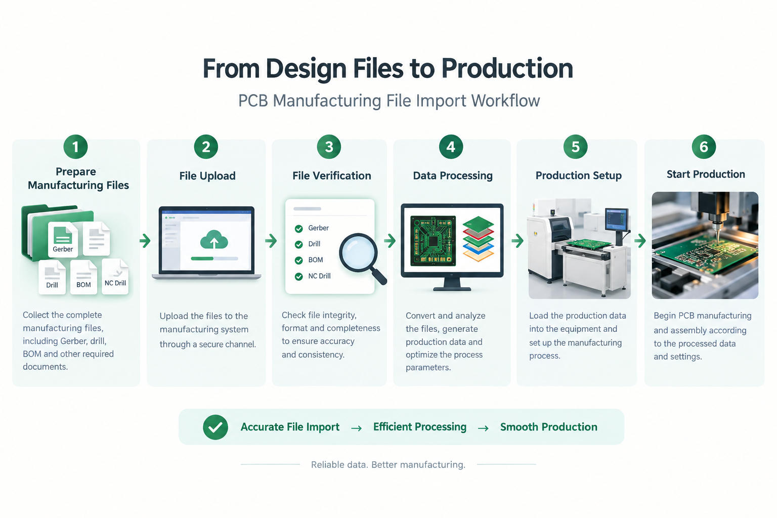
A PCB Manufacturing Package Usually Contains More Than Gerber
Sending the Gerber files is an important step, but it does not necessarily describe every requirement for manufacturing the board.
Drill data is one of the main additions.
PCB holes are generally supplied through NC drill data, often associated with the Excellon format. This data tells the manufacturer where holes are located and what sizes are required.
That matters for more than through-hole components. Vias, mounting holes, slots, and other drilled or routed features also have to be considered according to the manufacturing process.
The manufacturer may also need a fabrication drawing or other documentation covering specifications that cannot be understood simply by looking at the copper artwork.
Typical examples include:
| Information |
Why It Matters |
| Board thickness |
Determines the finished mechanical thickness |
| Copper thickness |
Affects current carrying capability and fabrication |
| PCB material |
Defines the base material used for the board |
| Surface finish |
Specifies the required finish on exposed copper |
| Layer stack-up |
Defines how a multilayer PCB is constructed |
| Board dimensions |
Used for mechanical processing and verification |
| Impedance requirements |
Important for controlled-impedance designs |
| Tolerances |
Defines acceptable dimensional variation |
Not every project needs a separate document for every item. Some information can be included through manufacturing data or the manufacturer's ordering system. The key is that the requirements are clear and unambiguous.
Gerber's Job File is another example of how manufacturing information can accompany Gerber data. It can communicate information such as board thickness, material and finish rather than trying to encode everything into the layer artwork itself.
What are the differences between Gerber, ODB++, and IPC-2581?
Gerber is not the only option.
If you have worked with larger or more complex PCB projects, you may have come across ODB++ or IPC-2581.
The main difference is the way information is organized.
Gerber traditionally handles PCB fabrication as a set of layer-based data files. Other formats can package a broader range of design and manufacturing information into a more structured data set.
|
Gerber |
ODB++ |
IPC-2581 |
| Layer information |
Yes |
Yes |
Yes |
| Drill information |
Usually separate data |
Can be included |
Can be included |
| Stack-up information |
Usually provided separately or through related data |
Supported |
Supported |
| Assembly information |
Usually separate |
Supported |
Supported |
| Data structure |
Layer-based |
Structured |
Structured |
IPC-2581 is an open standard developed for exchanging PCB and PCB assembly information. The standard is designed to carry data used in manufacturing, assembly and inspection rather than only describing individual PCB images.
ODB++ follows a similar idea of putting more manufacturing-related information into a structured data set.
That does not mean Gerber has become obsolete.
A PCB factory's preferred format depends on its manufacturing software, CAM workflow and the type of project being produced. A format that works well for one manufacturer may not be the preferred option for another.
For this reason, it is better to ask the manufacturer what files they accept before exporting the final production package.
What Should You Check Before Sending the Files?
A file can open correctly and still contain a manufacturing problem.
This is why checking the complete package is more useful than simply checking whether the files were exported successfully.
Start with the layer count.
If the PCB is a six-layer design, make sure all six copper layers are present and correctly identified. The order of the layers should also agree with the intended stack-up.
Next, check the board outline. A missing or incorrect outline can cause trouble during routing or mechanical processing. Slots and cutouts deserve the same attention.
The drill data should then be compared with the actual PCB layout. Check the hole sizes and locations, and make sure plated and non-plated holes have been handled correctly for the project.
There is another check that is easy to overlook: revision control.
Imagine that the copper files belong to Revision B, while the drill file was exported from Revision A. Both sets of files may look perfectly normal when opened individually. Together, however, they describe two different versions of the board.
For production, that is a serious problem.
It is also worth checking the manufacturing specifications before the files are released. Board thickness, copper weight, surface finish, material, impedance requirements and special mechanical requirements should not be left open to interpretation.
What Files Are Needed for PCBA?
This is where PCB fabrication and PCBA assembly start to diverge.
A bare PCB manufacturer mainly needs information about the board itself. An assembly manufacturer also needs to know which components are going onto the board and where they belong.
A typical PCBA data package may therefore include:
-
PCB fabrication files
-
Bill of Materials (BOM)
-
Pick-and-Place or centroid data
-
Assembly drawings
-
Component-related information
-
Testing requirements, when applicable
The BOM identifies the components used in the assembly. Pick-and-Place data provides placement information for SMT components.
The exact requirements can vary. Some manufacturers may request additional information depending on the assembly process, component types, inspection method, or testing requirements.
This is also why sending only a Gerber package is not enough when requesting a complete PCBA assembly quotation.
If you are looking for a manufacturing partner that handles both PCB fabrication and assembly, you can learn more about PCB and PCBA Manufacturing Services from HRPCBA.
FAQ
Q: Is Gerber the standard file type for PCB manufacturing?
A: Gerber is one of the most widely used formats for PCB fabrication and has broad industry support. However, it is not the only manufacturing data format available.
Q: Can a PCB be manufactured from Gerber files alone?
A: Not necessarily. A complete production package may also require NC drill data, board specifications, fabrication information, stack-up details, or other project-specific requirements.
Q: Is an original PCB design file needed?
For many standard fabrication projects, the manufacturer works from exported manufacturing data rather than the native editable CAD file. Whether the original design file is required depends on the manufacturer's A: process and the project.
Q: What is the difference between Gerber and IPC-2581?
A: Gerber is commonly used as a set of layer-based fabrication data. IPC-2581 can carry a broader and more structured set of PCB and assembly information in a single standardized data format.
Q: Should I choose Gerber or ODB++?
A: There is no universal requirement to use one format for every PCB project. Check with the manufacturer first. If the factory has a preferred data format, following its established workflow can make the engineering review more straightforward.
Conclusion
For most conventional PCB fabrication projects, Gerber remains a practical and widely supported choice.
But a PCB is not manufactured from a file extension alone. The factory needs enough accurate information to understand the board's electrical layers, holes, dimensions, materials, stack-up and other production requirements.
For a simple PCB, that may mean a Gerber package, NC drill data and basic fabrication specifications. More complicated projects may use structured formats such as ODB++ or IPC-2581. PCBA projects require still more information because components and their placement have to be defined.
Before sending your files, check the layer set, drill data, board outline, manufacturing specifications and revision together. That final review is often more valuable than spending time debating which file format is "the best."
The most useful manufacturing file is ultimately the one that gives the PCB manufacturer clear, complete and consistent information about what needs to be built.




 PCB AssemblyHRPCBA is a PCBA China manufacturer offering high-quality PCB assembly services with full-process support, from design to assembly and testing.
 PCB ManufacturingHRPCBA is a leading PCB board manufacturer offering precision PCB fabrication services. Get high-quality boards with fast turnaround and competitive pricing
 CapabilitiesDiscover HRPCBA’s robust PCB capabilities in custom PCB manufacturing services, where we transform your ideas into high-quality, functional circuit boards.