Industrial electronics are often expected to work for long periods under demanding conditions. Whether used in factory automation, power equipment, or industrial control systems, a PCB may need to handle temperature changes, electrical noise, mechanical vibration, and continuous operation.
That makes industrial PCB design different from simply creating a circuit that works. Material selection, component placement, trace dimensions, thermal management, and manufacturing requirements all influence how the finished board performs.
So, what should engineers consider when designing a PCB for industrial applications? Let's look at the standards, design details, and manufacturing considerations that matter in real projects.
Ⅰ Start with the Actual Working Environment
Before opening PCB design software, engineers should understand where the board will be used and what conditions it needs to withstand.
For example, a control board installed in factory automation equipment may be exposed to continuous vibration and electrical noise. A PCB used in power equipment, on the other hand, may require more attention to current capacity, component temperature, and electrical insulation.
Before starting the layout, define several basic requirements:
-
Operating voltage and maximum current.
-
Normal and maximum operating temperatures.
-
Available installation space and mounting method.
-
Possible exposure to vibration, shock, moisture, or dust.
-
Expected service life and maintenance requirements.
These details influence almost every design decision, from material selection and copper thickness to component placement and board structure.
It is also worth checking the mechanical requirements early. If a connector is placed in the wrong position or the board does not fit the enclosure, changing the layout after completion can take considerably more time than addressing the issue during the initial design stage.
Ⅱ. Which Industrial Standards Should PCB Designers Know?
There is no single standard that covers every industrial PCB application. The applicable requirements depend on the product, customer specifications, manufacturing process, and target market.
Several industry standards are commonly referenced during PCB design, fabrication, and assembly.
| Standard |
Main Application |
| IPC-2221 |
Generic printed board design requirements |
| IPC-6012 |
Qualification and performance specifications for rigid printed boards |
| IPC-A-600 |
Acceptability of printed boards |
| IPC-A-610 |
Acceptability of electronic assemblies |
| UL 796 |
Safety-related requirements for printed wiring boards |
These standards serve different purposes.
IPC-2221 provides general guidance for printed board design. IPC-6012 focuses on the qualification and performance requirements of rigid printed boards, while IPC-A-600 is commonly used as a visual reference when evaluating bare PCB quality.
For assembled boards, IPC-A-610 provides acceptance criteria for electronic assemblies.
Designers should not assume that meeting one standard automatically means a product meets every industrial requirement. The applicable revision, product class, and acceptance criteria should be confirmed with the customer before production.
For products intended for markets with specific safety requirements, standards such as UL 796 may also need to be considered. The final requirements depend on the end product and its certification scope.
Ⅲ. Design Details That Make a Difference
3.1 Choose Materials Based on Operating Conditions
FR-4 is widely used in PCB manufacturing and works well for many conventional electronic applications. However, it is not necessarily the best choice for every industrial project.
Material selection should take operating temperature, thermal performance, dielectric properties, and mechanical requirements into account.
For example, a board operating at elevated temperatures may require an evaluation of high-Tg materials. High-frequency and high-speed applications may need materials with more suitable dielectric characteristics and lower signal loss.
The selected material should also be compatible with the intended lamination, drilling, and assembly processes. Choosing a material based only on price can create difficulties later if it does not match the product's operating or manufacturing requirements.
3.2 Calculate Trace Width and Spacing Properly
Trace width is directly related to current-carrying capacity, temperature rise, and voltage drop. For power circuits, narrow traces may cause excessive heating or unwanted voltage loss.
Instead of relying on a fixed trace width, engineers should calculate it based on current, copper thickness, allowable temperature rise, and the actual board construction.
Clearance requirements also deserve attention. The spacing between conductors depends on factors such as working voltage, insulation requirements, pollution conditions, and the applicable design standards.
For high-voltage circuits, electrical clearance and creepage distance should be evaluated separately. They are not interchangeable, and both may affect the final layout.
If controlled impedance is required, the designer should discuss the proposed stack-up and material properties with the PCB manufacturer. This helps ensure that the calculated impedance can be achieved during fabrication.
3.3 Think About Heat Before the Layout Is Finished
Power components are often the main heat sources on industrial control and power boards. Placing several high-power devices too close together can create localized hot spots, even when the circuit operates normally during initial testing.
A few practical considerations can help:
-
Leave appropriate space between major heat-generating components.
-
Use copper areas to help spread heat.
-
Consider thermal vias where the board structure allows them.
-
Keep temperature-sensitive components away from major heat sources.
-
Evaluate the PCB together with the enclosure and external cooling structure.
Adding more copper or thermal vias does not automatically solve every thermal problem. The actual result depends on component power, copper distribution, layer structure, material properties, and the surrounding cooling conditions.
For demanding applications, thermal simulation or physical temperature testing may be necessary.
3.4 Layout and Routing Affect Reliability
Electrical performance is not determined by trace width alone. Component placement, grounding, and signal routing also influence how a PCB behaves in a real operating environment.
For example, switching power circuits placed too close to sensitive analog circuits may introduce unwanted noise. Poor return paths can also contribute to electromagnetic interference and signal integrity problems.
Engineers should pay attention to:
-
Ground plane continuity and return current paths.
-
Separation between noisy power circuits and sensitive signals.
-
Appropriate routing for high-speed interfaces.
-
Impedance control and differential pair requirements.
-
Mechanical stress around mounting holes and connectors.
For high-speed signals, routing rules should follow the requirements of the specific interface rather than relying on general layout habits.
Mechanical design matters as well. Mounting holes, board edges, and connector positions should match the enclosure and assembly method. Otherwise, the finished PCB may experience unnecessary stress during installation or operation.
Ⅳ. A Design Must Also Be Practical to Manufacture
A PCB may pass the checks in design software but still encounter problems during fabrication or assembly. In many cases, the issue comes from a mismatch between the design and the manufacturer's actual process capabilities.
This is where DFM (Design for Manufacturability) becomes important.
For example, incorrect pad dimensions, insufficient component spacing, unsuitable hole sizes, or limited process clearance around BGA packages may increase manufacturing difficulty.
Before releasing the design, review the following items:
-
Whether board thickness, copper thickness, and hole sizes match the manufacturing requirements.
-
Whether trace spacing and pad dimensions are appropriate.
-
Whether component footprints match the actual parts in the BOM.
-
Whether BGA and fine-pitch components allow for the intended assembly process.
-
Whether Gerber files, drill files, BOM data, and pick-and-place coordinates are consistent.
For projects involving both PCB fabrication and PCBA assembly, it is better to discuss these details with the manufacturer before production.
A manufacturing review at this stage can identify problems that may not be obvious during the layout process.
If you are preparing your first production files, you may also find this guide useful: How to Create PCB Designs from Scratch?. It covers the basic process from design requirements to manufacturing file preparation.
Ⅴ. How Can You Verify PCB Quality?
Design review is only the beginning. Once the board enters fabrication and assembly, appropriate inspection and testing are needed to check whether the finished product meets the project requirements.
Different testing methods serve different purposes.
| Testing Method |
What It Checks |
| AOI |
Visible circuit and soldering defects |
| Flying Probe Test |
Electrical connections on bare PCBs |
| X-ray Inspection |
Hidden solder joints, including BGA connections |
| ICT |
Electrical characteristics of assembled boards |
| Functional Testing |
Actual product functions under defined test conditions |
For example, AOI can identify visible assembly defects and component placement issues, but it cannot replace all electrical tests. X-ray inspection is useful for examining solder joints that cannot be seen directly, while functional testing checks whether the assembled product performs as intended.
For industrial projects, prototype validation is particularly useful. Testing early samples can reveal design, fabrication, or assembly problems before the project moves into volume production.
Not every project needs every inspection method. The test plan should reflect the board structure, component package types, product risks, and customer requirements. Acceptance criteria and test records should also be agreed upon before production.
Ⅵ. Choosing the Right PCB Manufacturing Partner
The relationship between PCB design and manufacturing is closer than many people expect. A supplier's ability to understand technical requirements and identify production issues can make a real difference to an industrial project.
A suitable manufacturing partner should do more than receive design files and produce circuit boards. Communication about manufacturability, assembly requirements, and quality expectations should take place before production begins.
HongRong (Shenzhen) Electronics Co., Ltd. provides PCB manufacturing and PCBA assembly services, supporting customers who need a one-stop solution from bare board production to electronic assembly.
For projects that require additional manufacturing review, early communication and DFM checks can help identify file issues and process mismatches before they lead to rework.
According to the quality information published on the HRPCBA website, its quality control process includes AOI, X-ray, ICT, functional testing, and aging testing. The inspection plan for an individual project should be confirmed according to its product requirements and agreed testing arrangements.
If you are looking for PCB fabrication or assembly support, you can learn more about HRPCBA's PCB and PCBA services and its quality control and technical support.
Ⅶ. Conclusion
Designing a PCB for industrial applications is not simply a matter of using thicker copper, selecting a higher-grade material, or adding more inspection steps.
What matters is making sure that the design matches the product's operating environment, electrical requirements, and manufacturing conditions.
Material selection, trace design, thermal management, mechanical layout, and DFM review all contribute to the performance of the finished board. Overlooking one of these areas may create problems that are difficult and expensive to correct later.
For industrial electronics projects, communication between the design team and the PCB manufacturer should start early. It is usually more practical to address manufacturing concerns during design than to discover them after production has begun.
HongRong provides PCB manufacturing and PCBA assembly support to help customers move their projects from design files toward actual production.




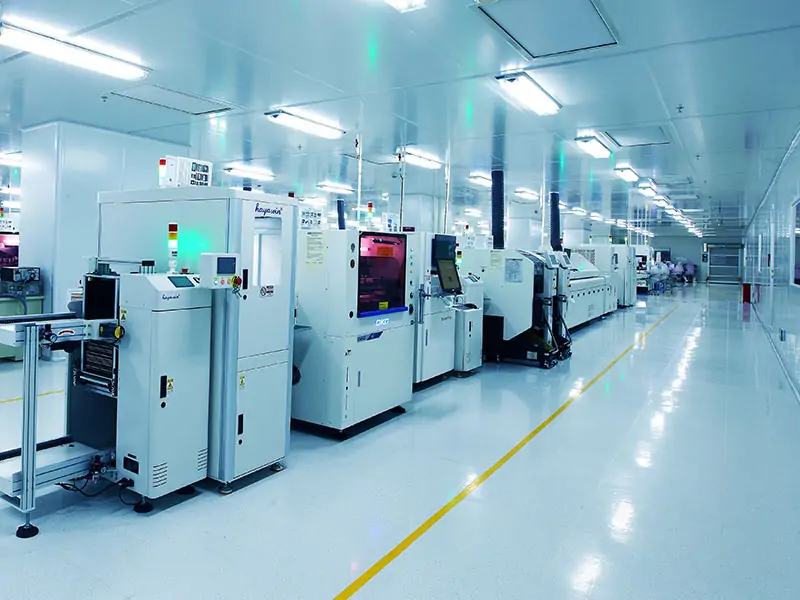
 PCB AssemblyHRPCBA is a PCBA China manufacturer offering high-quality PCB assembly services with full-process support, from design to assembly and testing.
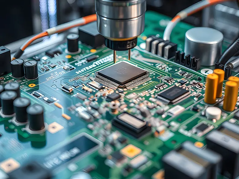
 PCB ManufacturingHRPCBA is a leading PCB board manufacturer offering precision PCB fabrication services. Get high-quality boards with fast turnaround and competitive pricing
 CapabilitiesDiscover HRPCBA’s robust PCB capabilities in custom PCB manufacturing services, where we transform your ideas into high-quality, functional circuit boards.