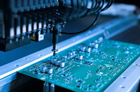
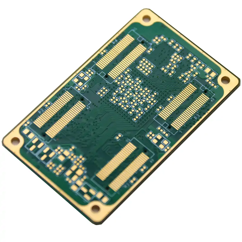
When you open a smart home device, an industrial controller, or even a smartphone, the most noticeable component is often not the processor—it's the printed circuit board (PCB).
Although it may look like a simple board that holds electronic components, a PCB plays a much bigger role. It determines how reliably electrical signals travel, how efficiently heat is managed, and how easily the product can be manufactured and assembled. Even with a perfectly designed schematic, poor PCB layout can still lead to unstable performance, excessive electromagnetic interference (EMI), or expensive redesigns.
Many beginners assume PCB design is difficult because it involves electronics, CAD software, manufacturing rules, and signal integrity. In reality, professional PCB design follows a structured engineering workflow. By understanding each step and the reason behind it, anyone can gradually build the skills needed to design production-ready circuit boards.
This guide walks through the complete PCB design process—from defining project requirements to preparing manufacturing files—while sharing practical design considerations used in real engineering projects.
If your project will eventually move into PCB fabrication and assembly, understanding manufacturing requirements early can save both time and cost. You can also explore the one-stop PCB manufacturing and assembly solutions offered by HRPCBA at https://www.hrpcba.com.
What Is PCB Design?
One of the most common misunderstandings among beginners is believing that a completed schematic means the design is finished.
A schematic only defines the electrical relationships between components. PCB design takes those logical connections and turns them into a physical circuit board that can actually be manufactured and assembled.
In simple terms, the schematic answers "What should be connected?", while PCB layout answers "How should those connections be implemented in the real world?"A well-designed PCB is more than a collection of traces. It also considers thermal performance, manufacturability, assembly efficiency, electromagnetic compatibility (EMC), and long-term reliability. That is why PCB design is often viewed as the bridge between electronic design and manufacturing.
Schematic Design vs. PCB Layout
| Schematic Design |
PCB Layout |
| Defines electrical connections |
Creates the physical board layout |
| Focuses on circuit functionality |
Focuses on manufacturability and performance |
| Produces the netlist |
Generates Gerber, drill, and manufacturing files |
| Validates circuit logic |
Optimizes routing, EMC, and assembly |
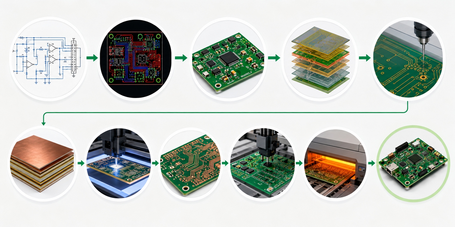
A typical electronics development process looks like this:
Product Requirements → Circuit Design → Schematic → PCB Layout → PCB Fabrication → PCB Assembly → Functional Testing
PCB layout sits at the center of this workflow. Decisions made during the design stage often determine how smoothly the product moves into manufacturing and how reliable it performs in real-world applications.
Step 1: Define Your Design Requirements
Experienced PCB designers rarely start by opening their PCB software.
Instead, they spend time understanding the project requirements first. This early planning often prevents costly design revisions later.
For example, changing the enclosure size, moving connectors, or adding new functions after the PCB layout has already begun can significantly increase development time.
Before creating your PCB, ask yourself a few basic questions:
- What functions should the product perform?
- What are the operating voltage and current?
- Will it include high-speed interfaces such as USB or DDR?
- How much board space is available?
- What environmental conditions will the product operate in?
The answers to these questions influence nearly every design decision that follows, from board stack-up to component placement and routing strategy.
Step 2: Choose the Right PCB Stack-up
A PCB does not necessarily perform better with more layers, nor is it always more cost-effective with fewer layers. Selecting the appropriate number of PCB layers requires a comprehensive consideration of circuit complexity, signal integrity, EMI control, and the project budget.
The following are common PCB layer counts and their typical applications.
| PCB Type |
Typical Applications |
Features |
| Single-sided PCB |
Simple control boards, LED lighting |
Lowest cost, limited routing capability |
Double-sided PCB
|
Consumer electronics, industrial control |
Widely used, suitable for products of low to medium complexity |
| 4-Layer PCB |
MCU development boards, communication equipment, embedded systems |
Addition of power and ground layers helps improve signal integrity |
| 6-Layer (and higher) PCB |
High-speed communication, servers, automotive electronics |
Better EMI control and higher routing density; suitable for complex designs |
For most small and medium-sized electronic products, two-layer and four-layer PCBs remain the most common choices. Four-layer boards typically offer more complete power and ground planes, which helps reduce noise, optimize high-speed signal transmission, and enhance overall electrical performance.
Step 3: Create the Schematic
Once the project requirements are clear, the next step is creating the schematic.
Think of the schematic as the logical blueprint of your circuit. It defines how components are electrically connected, but it does not determine where they will be placed on the PCB. A well-organized schematic makes the entire design process easier, especially when multiple engineers are involved.
A practical approach is to organize the design into functional blocks, such as the power supply, MCU, communication interfaces, and peripheral circuits. This structure simplifies future revisions and provides a solid foundation for PCB layout.
Before moving to the layout stage, run an Electrical Rule Check (ERC). ERC helps identify common issues such as floating pins, duplicate net names, or incorrect power connections. While it cannot catch every design mistake, it significantly reduces the chance of carrying basic errors into the PCB layout.
For experienced engineers, a schematic is more than just a design document—it also serves as an important reference for debugging, production, and long-term maintenance.
Step 4: Select the appropriate component footprints (Assign the Right PCB Footprints)
After the schematic is complete, each component must be assigned the correct PCB footprint.
Although this step may seem straightforward, footprint mismatches remain one of the most common reasons for PCB redesigns. The same integrated circuit may be available in packages such as SOIC, TSSOP, or QFN, and selecting the wrong footprint can prevent the board from being assembled successfully.
When choosing a footprint, verify not only the package type but also pad dimensions, pin spacing, and orientation. For high-density packages like QFN or BGA, using verified manufacturer libraries is generally safer than creating custom footprints from scratch.
If the board will eventually be assembled using automated SMT production, selecting footprints that follow standard manufacturing guidelines will help improve assembly quality and reduce production risks.
Step 5: PCB Placement
Many engineers believe routing is the most challenging part of PCB design. In practice, good routing often begins with good component placement.
A carefully planned layout shortens critical signal paths, reduces interference, and leaves enough room for clean routing. Investing more time in placement usually saves time during the routing stage.
Some practical placement guidelines include:
- Group components according to their functions.
- Keep power circuits close to the loads they supply.
- Place decoupling capacitors as close as possible to IC power pins.
- Minimize the distance between high-speed components.
- Position connectors such as USB, RJ45, or HDMI near the board edge whenever possible.
Thermal management should also be considered during placement. Spreading high-power devices appropriately helps improve heat dissipation and contributes to long-term reliability.
There is no universal placement template, but following these engineering principles provides a strong foundation for the rest of the PCB design.
Step 6: PCB Routing
With component placement complete, the next step is routing.
Routing is more than simply connecting every net. The goal is to ensure signals travel accurately and reliably while maintaining good electrical performance. For standard control boards, following fundamental routing practices is often sufficient. High-speed designs, however, require additional attention.
Some widely accepted routing guidelines include:
| Recommendation |
Why It Matters |
| Keep signal paths as short as practical |
Reduces delay and unwanted inductance |
| Avoid sharp 90° corners |
Improves manufacturability and signal continuity |
| Maintain a continuous ground plane |
Reduces EMI and provides a better return path |
| Match the lengths of high-speed signals |
Helps maintain signal integrity |
| Use wider traces for power rails |
Reduces voltage drop and heat generation |
For interfaces such as USB, DDR, PCIe, or other high-speed buses, designers should also consider impedance control, differential pair routing, and length matching according to the PCB manufacturer's capabilities.
If your design is intended for production, discussing manufacturability with your PCB supplier before fabrication can help minimize revisions and improve production efficiency. More information about PCB fabrication and assembly services is available on the HRPCBA website: https://www.hrpcba.com
Step 7: Run Design Rule Checks
Before generating manufacturing files, perform a final design review.
Most EDA tools include Design Rule Check (DRC) to detect issues such as clearance violations, short circuits, open nets, and incorrect pad spacing.
Besides DRC, it is worth reviewing:
- Component orientation
- Power and ground planes
- High-speed signal routing
- Silkscreen placement
- Thermal clearance
A few minutes spent reviewing the design can prevent costly revisions later.
Step 8: Generate Manufacturing Files
After the design is verified, export the manufacturing files.
For PCB fabrication, Gerber and drill files are required. If PCB assembly is included, prepare the BOM, Pick-and-Place file, and Assembly Drawing as well.
| File |
Purpose |
| Gerber |
PCB artwork |
| Drill File |
Hole information |
| BOM |
Component list |
| Pick and Place |
SMT coordinates |
| Assembly Drawing |
Assembly reference |
Review the exported files before sending them to the manufacturer to avoid unnecessary delays.
Step 9: Move to PCB Fabrication and Assembly
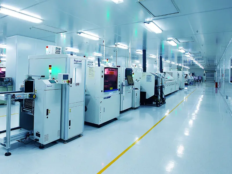
Once the design is released, the project moves into PCB fabrication and assembly, including PCB manufacturing, SMT placement, reflow soldering, AOI inspection, and functional testing.
Good PCB design improves production efficiency, while poor layout or footprint selection may lead to assembly issues.
If your board is intended for mass production, discussing DFM requirements with your manufacturer early is recommended.
Common PCB Design Mistakes
Many PCB issues are caused by overlooked details rather than complex engineering problems.
| Common Mistake |
Impact |
| Decoupling capacitors placed too far away |
Increased power noise |
| Narrow power traces |
Higher voltage drop |
| Broken ground plane |
Increased EMI |
| Unequal high-speed trace lengths |
Poor signal integrity |
| Silkscreen on pads |
Assembly issues |
| Skipping DRC |
Higher risk of redesign |
Following a structured review process helps improve both reliability and manufacturability.
Best Practices for PCB Design
For beginners, mastering good design habits is more important than tackling complex high-speed circuits.
A few practical recommendations include:
- Define the project requirements before starting the layout.
- Organize components by functional blocks.
- Use verified component footprints.
- Run ERC and DRC after every major revision.
- Consider manufacturing and assembly requirements early in the design process.
A structured workflow improves both design quality and production e
fficiency.
FAQ
Q1: Should beginners start with a 2-layer or 4-layer PCB?
A 2-layer PCB is suitable for most beginner projects, while a 4-layer board offers better signal integrity and routing flexibility for more complex designs.
Q2: Can a PCB be manufactured immediately after the layout is finished?
Not yet. Always complete ERC, DRC, and a final design review before releasing the manufacturing files.
Q3: Which software is commonly used for PCB design?
Popular PCB design tools include KiCad, Altium Designer, Autodesk Eagle, and OrCAD. Choose the one that best fits your project requirements.
Conclusion
PCB design is much more than connecting electronic components. It bridges the gap between circuit design and manufacturing, and every stage—from project planning to manufacturing file generation—affects the final product's performance and reliability.
For beginners, following a structured design process is far more valuable than focusing on advanced techniques. As your experience grows, so will your ability to create efficient, reliable, and manufacturable PCB designs.
If your project is ready for fabrication or PCB assembly, visit HRPCBA to learn more about its one-stop PCB manufacturing, component sourcing, and PCB assembly services. https://www.hrpcba.com




 PCB AssemblyHRPCBA is a PCBA China manufacturer offering high-quality PCB assembly services with full-process support, from design to assembly and testing.
 PCB ManufacturingHRPCBA is a leading PCB board manufacturer offering precision PCB fabrication services. Get high-quality boards with fast turnaround and competitive pricing
 CapabilitiesDiscover HRPCBA’s robust PCB capabilities in custom PCB manufacturing services, where we transform your ideas into high-quality, functional circuit boards.