High-Density Interconnects (HDI) have become a core part of today’s electronics industry. Devices are getting smaller, faster, and more advanced, which increases the need for PCB layouts that support tight spacing, stable routing, and high-speed performance. That is why HDI, PCB design, signal integrity play a major role in developing reliable products for industries like consumer electronics, medical engineering, communication systems, industrial control equipment, and automotive electronics. In this detailed guide, you will learn what HDI means, how it helps improve product performance, why it matters for HDI, PCB design, signal integrity, and what engineers must consider during development.
What Are High-Density Interconnects (HDI) and Why They Matter for HDI, PCB Design, Signal Integrity
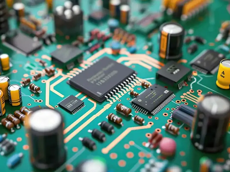
High-Density Interconnects refers to circuit boards with high wiring density per unit area. HDI supports fine wiring, microbias, build-up layers, and compact wiring routes. These boards provide more freedom for designers working with advanced chips, small components and high-speed signals. HDI is important because modern electronic products rely on small parts and high-speed data communication. Even if the size is reduced and the function is improved, the PCB must continue to process the load without compromising performance. HDI, PCB design and signal integrity are essential here.
Key points that show the importance of HDI in the industry:
- HDI supports smaller devices without losing performance.
- It improves signal paths, which helps keep HDI, PCB design, signal integrity stable.
- It handles high-speed processors and memory chips.
- It improves thermal performance and reliability.
- Helps reduce electromagnetic interference.
HDI substrates are a major requirement for devices such as smartphones, tablets, medical sensors, and automotive control systems.
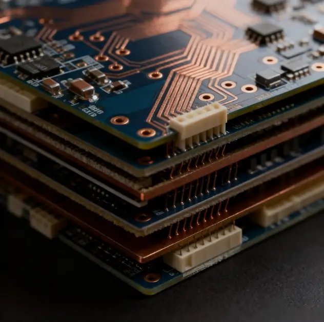
Types of HDI and Their Role in HDI, PCB Design, Signal Integrity
HDI PCBs come in different structures. Each type supports unique applications and affects HDI, PCB design, signal integrity in different ways. The main types include:
1. Through Vias from Surface to Surface
These HDI boards use standard vias that connect the top and bottom layers. They are simple but effective for basic routing needs. This type supports stable paths and helps maintain HDI, PCB design, signal integrity in products that do not require complex layer structures.
2. Buried Vias and Through Vias
This structure combines internal buried vias with standard through vias, giving more routing freedom. It reduces congestion and allows cleaner signal movement. Because of the improved layer connection, it strengthens HDI, PCB design, signal integrity in devices with higher component density and multi-layer routing.
3. Multiple HDI Layers with Through Vias
Boards with multiple HDI layers allow designers to handle complex circuits and high-speed chips. They support tighter spacing, shorter paths, and improved signal control. This structure offers strong reliability, making it ideal for advanced products that depend on stable HDI, PCB design, signal integrity.
4. Passive Substrates with No Electrical Connections
These HDI structures do not carry signals but are used for added strength, heat control, or mechanical support. They help manage board stability in very compact devices. Even without active routing, they indirectly support better HDI, PCB design, signal integrity by improving the board’s physical performance.
5. Coreless Construction Using Layer Pairs
Coreless HDI boards remove the central core and use thin layer pairs instead. This reduces board thickness and supports fine-pitch components. The lightweight structure helps maintain stable routing paths and boosts HDI, PCB design, signal integrity in miniaturized and portable electronic devices.
6. Alternate Coreless Layer Constructions
This type uses multiple coreless layers arranged in alternating patterns. It supports high-speed circuits, flexible routing, and very tight spacing. Because of its advanced design, it is often used in compact products that demand strong HDI, PCB design, signal integrity for stable operation and clean signal flow.
Each type increases design flexibility and supports products with strict requirements for size, speed, and performance.
How HDI Improves HDI, PCB Design, Signal Integrity in Modern Electronics
Signal integrity plays a major role in every PCB. When signals move across the board, they must stay clean, stable, and accurate. HDI helps maintain this through several ways:
1. Shorter Signal Paths
HDI boards offer short and straight routing lines. Shorter paths reduce delays, noise, and interference. This helps maintain HDI, PCB design, signal integrity in communication circuits and high-speed processors.
2. Lower Layer Count with Better Results
Even with fewer layers, HDI can carry more data. This reduces board thickness while keeping HDI, PCB design, signal integrity strong.
3. Reduced Electromagnetic Problems
HDI layouts reduce cross-talk and radiation issues. This is essential in medical devices, automotive electronics, and wireless systems.
4. Better Thermal Performance
Heat can damage circuits and affect signal flow. HDI helps dissipate heat and keep the system stable during long operation.
Because of these advantages, HDI PCBs are now used in almost every high-performance electronic device.
Key Design Rules for HDI, PCB Design, Signal Integrity
HDI design requires careful planning. Because everything is smaller, engineers need to follow certain rules to protect HDI, PCB design, signal integrity and ensure stable operation.
1. Controlled Impedance Routing
Many modern circuits depend on stable impedance. HDI layouts can support accurate impedance control on high-speed lines.
2. Microvia Placement
Microvias must be placed correctly to avoid cracks, failure points, or stress. Their quality directly affects HDI, PCB design, signal integrity.
3. Layer Stack-Up
Choosing the best stack-up is essential. A good stack-up helps reduce noise, improve stability, and support high-speed components.
4. Component Spacing
Even though HDI reduces spacing, certain standards must be maintained to avoid short circuits or thermal buildup.
5. Via-in-Pad for High-Speed Signals
Via-in-pad allows signals to move directly from component pads into vias. This improves routing and helps keep HDI, PCB design, signal integrity stable.
Following these rules helps engineers create boards that run well under pressure and maintain signal quality.
Applications of HDI and Their Link to HDI, PCB Design, Signal Integrity
HDI is now used across multiple industries because it supports high-speed, compact, and long-lasting devices.
1. Consumer Electronics
Smartphones, tablets, cameras, laptops and wearable devices all rely on HDI. These products require strong HDI, PCB design and signal integrity for high-speed data transfer and stable use.
2. Communication Equipment
Routers, network switches, wireless devices, and 5G systems rely on HDI because they need stable high-frequency routing.
3. Medical Equipment
Compact medical sensors and diagnostic tools use HDI for reliability and accuracy.
4. Automotive Electronics
ADAS, sensors, cameras and infotainment systems require stable HDI, PCB design and signal integrity. Automotive electronics operate in harsh environments.
5. Industrial Equipment
Robotics, automation systems, and machine controllers use HDI to support stable signals across long operation cycles.
HDI PCB Board: High-Density Interconnect PCB (HRPCBA Overview)
If you are searching for a trusted HDI manufacturer, HRPCBA delivers high-quality HDI boards designed for stable HDI, PCB design, signal integrity across modern devices. HRPCBA manufactures all major HDI structures, including through vias, buried vias, microvia build-ups, coreless HDI, and advanced multi-layer systems. These boards support compact layout, fast wiring, and long-term reliability. HRPCBA's solutions are widely used in consumer electronics, medical devices, automotive electronics and industrial equipment, making them the best choice for projects that require accuracy and stable performance.
Key Features
- Supports compact layouts for small devices while keeping routing clean and stable for strong HDI, PCB design, signal integrity.
- Offers microvia and buried-via structures that improve high-speed signal flow and reduce noise across dense components.
- Provides stable heat control that helps the board run smoothly during long operation in sensitive applications.
- Delivers accurate multi-layer stack-ups that support advanced chips, processors, and complex connection paths.
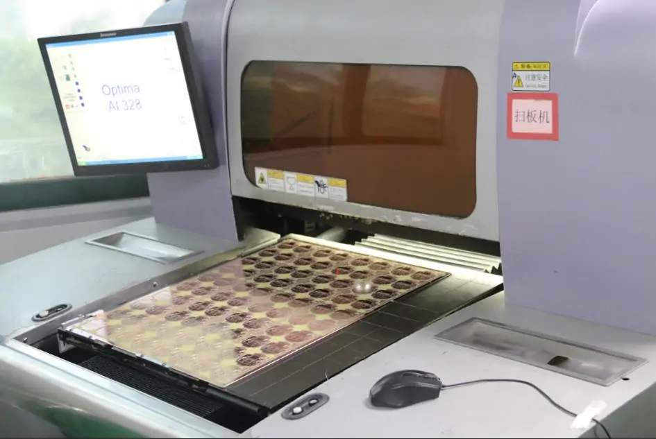
- Ensures reliable manufacturing quality with detailed testing, helping products maintain long-term HDI, PCB design, signal integrity.
Conclusion
HDI technology has become essential for modern electronic products. Improves wiring efficiency, enhances HDI, PCB design, signal integrity, reduces board size and supports high-speed functions. As devices continue to become smaller and more sophisticated, HDI PCB will continue to be the core of its design. If you want dependable manufacturing, professional support, and strong board performance, you can trust HRPCBA. Their HDI PCB services provide accurate production, strong signal quality, and reliable results for different industries. You can visit their HDI PCB page or contact them for a quote to support your next project.


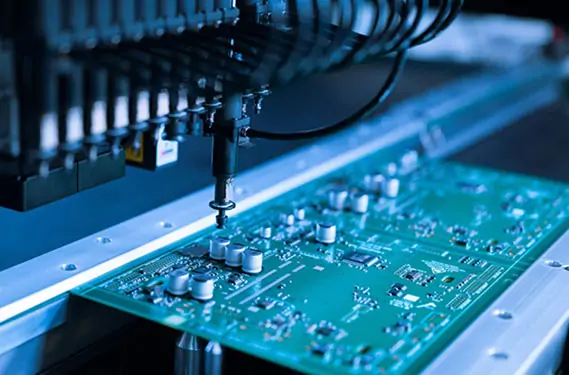
 PCB AssemblyHRPCBA is a PCBA China manufacturer offering high-quality PCB assembly services with full-process support, from design to assembly and testing.
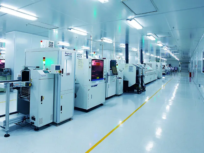 PCB ManufacturingHRPCBA is a leading PCB board manufacturer offering precision PCB fabrication services. Get high-quality boards with fast turnaround and competitive pricing
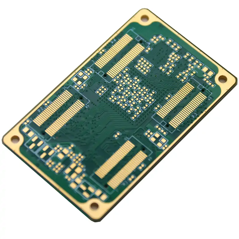
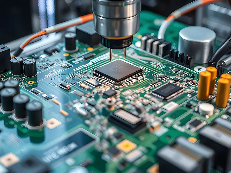 CapabilitiesDiscover HRPCBA’s robust PCB capabilities in custom PCB manufacturing services, where we transform your ideas into high-quality, functional circuit boards.