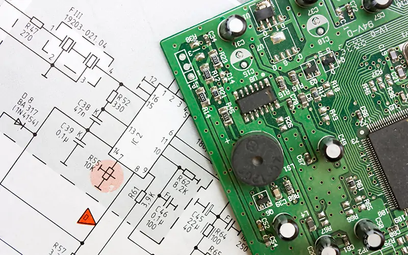
Printed circuit boards (PCBs) are essential components for almost all electronic devices, from smartphones to computers. These substrates serve as the basis for connecting electronic components such as resistors, capacitors, microchips, and connectors to make them function smoothly. PCB prototyping is an important step in electronics development, regardless of beginner, hobbyist or experienced engineer. Prototyping is the process of creating a test version of a PCB to check whether the design works properly before mass production begins. This guide briefly describes the key elements of PCB prototyping. It includes processes, materials, and common techniques often used to create these important substrates.
What is PCB Prototyping?
PCB prototyping is the process of creating a test version of a PCB. This prototype is used to check if the design works before mass production starts. The purpose of prototyping is to ensure that the design works as expected, that all connections are in the right position and that the layout works properly on the intended device. PCB prototyping plays an important role in electronics development. Because designers can identify problems early in the process, they can save time and money in the long run.
Why is PCB Prototyping Important?
There are a number of reasons why prototyping is crucial:
- Error Detection: Minor design errors may also lead to major issues. Prototyping ensures that you detect and rectify errors prior to final production.
- Design Validation: Ensure that the circuit design is functional as per plan under real usage conditions.
- Cost-Effective: Testing of the prototypes before mass production avoids the production of defective designs, hence cost savings.
- Faster Development: Discovery of errors early ensures timely change, leading to speeding up of end production
The PCB Prototyping Process
The PCB prototyping process is generally made up of several steps. The most common stages are discussed below:
1. Designing the PCB
The first step of PCB prototyping is circuit design. It's normally done using computer-aided design (CAD) software to create an electronic copy of the PCB. Popular PCB design tools are Eagle, KiCad, and Altium Designer.
During design, we do the following:
- Layout the Components: Place on the board all the components required, including capacitors, resistors, microchips, and connectors.
- Route the Traces: This is the electronic path that supplies wires between devices.
- Check for Errors: Most contemporary software comes equipped with error detection to check if the design functions.
2. Printing the PCB Design
Once designed, then create a physical copy. This usually involves the process of printing the design on copper foil substrates. Copper foil substrates are substrates employed in producing circuits through etching later.
The process is as follows:
- Printing the Design: Print the design onto the copper surface using UV exposure or toner transfer.
- Etching: Spools off excess copper and leaves traces and pads behind that connect components.
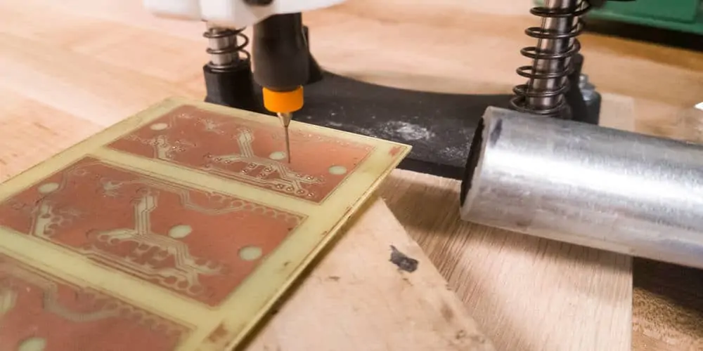
3. Drilling the Holes
PCB has holes for mounting and connecting components. Holes are drilled in areas marked in the design. Holes can also be used as vias to interconnect different layers of PCB.
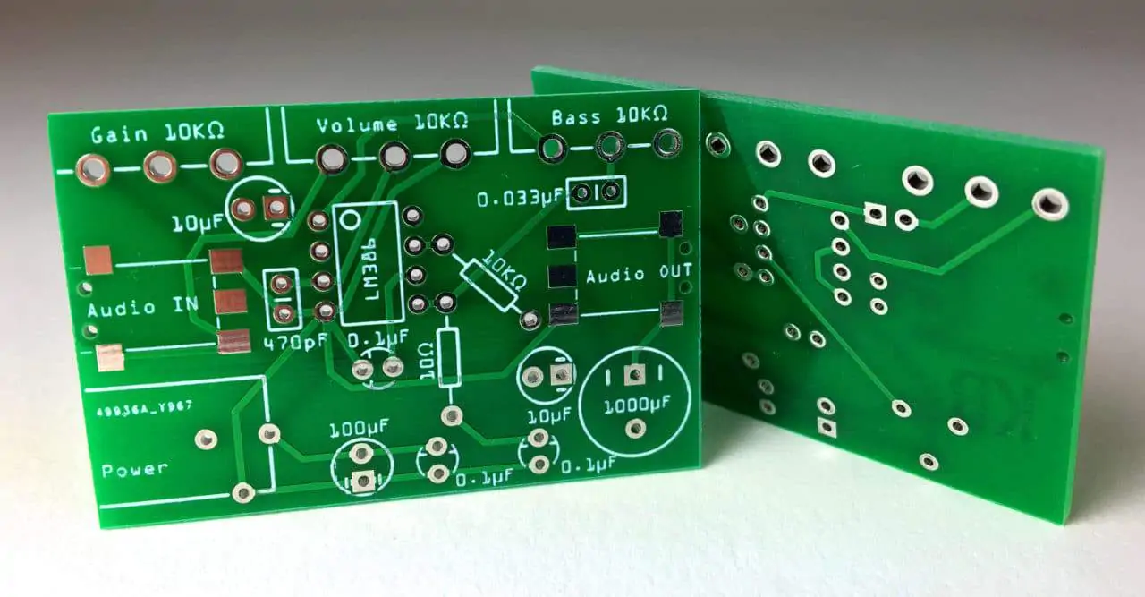
4. Applying Solder Mask and Silkscreen
Solder masks protect components from copper traces and prevent short circuits when soldering. By exposing only pads (areas) that solder components, they also prevent short circuits accidentally during soldering. After the solder mask layer, the silk screen layer is applied, revealing the component's marking and orientation on the board.
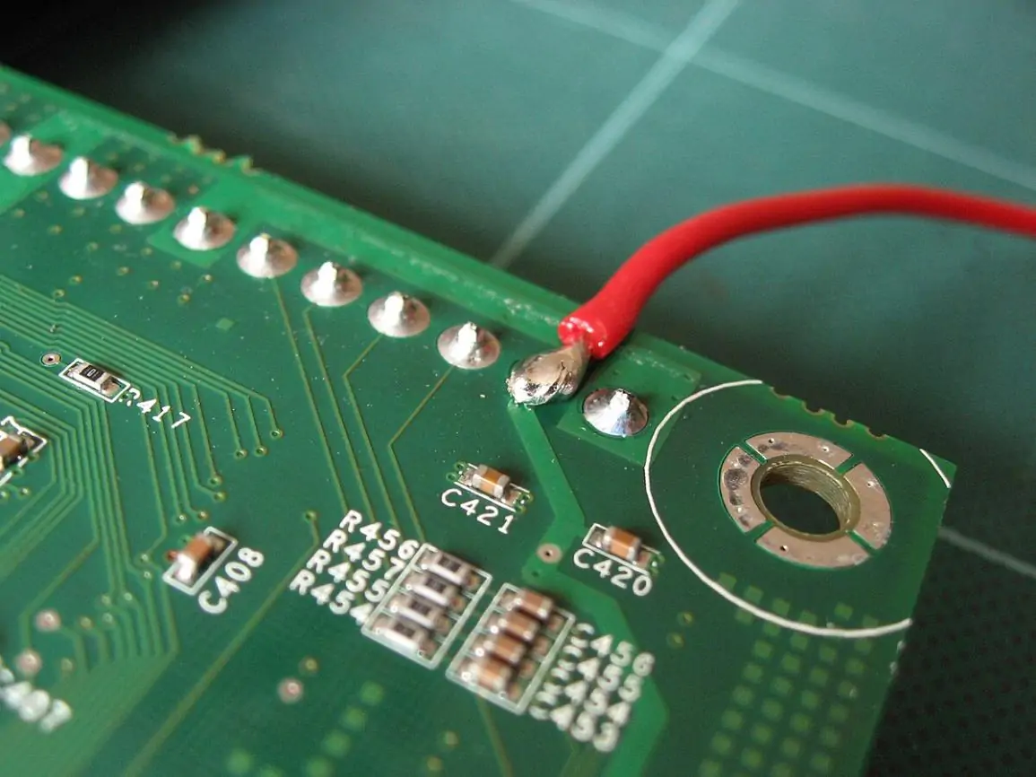
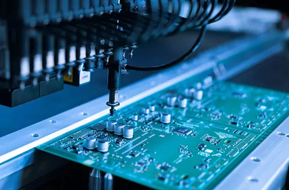
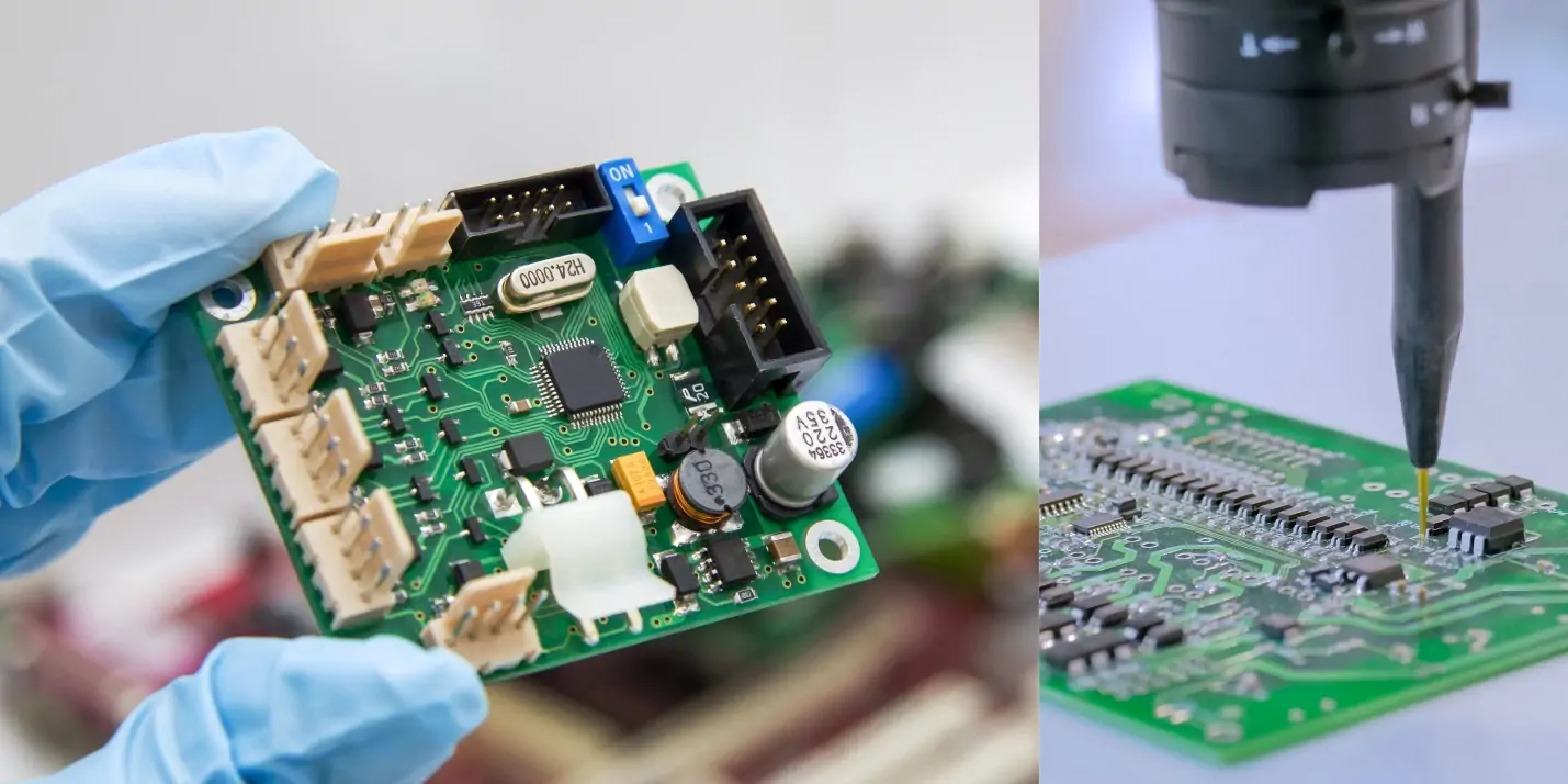
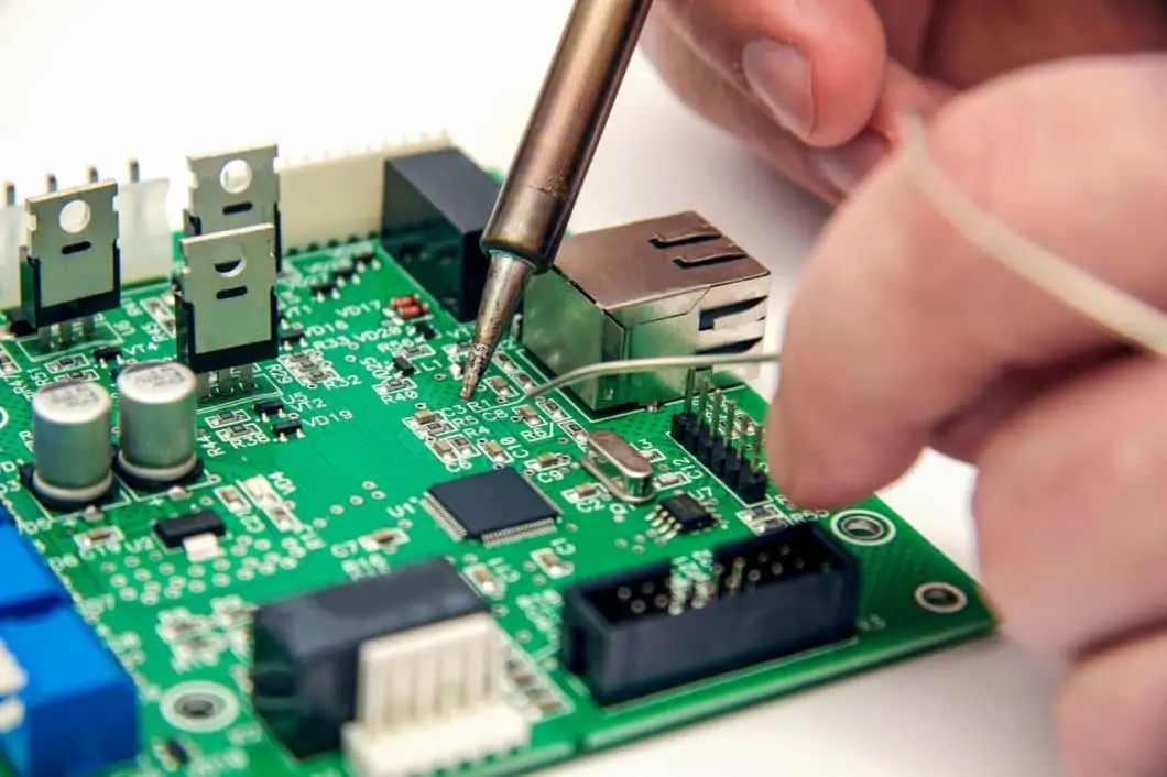
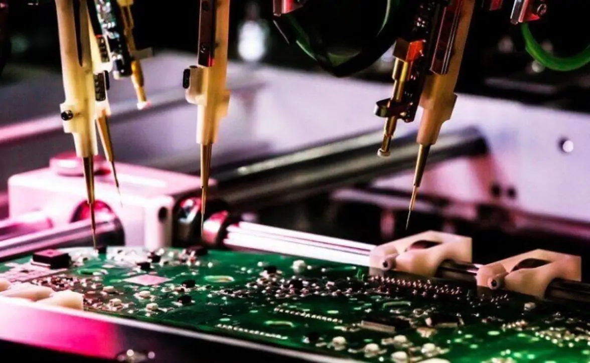
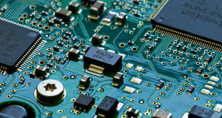
5. Component Placement and Soldering
When the PCB is ready, now is the time to mount the component. In doing so, all components are soldered on the PCB safely and placed in their correct position. When in small quantities, it is done manually and when producing in bulk, it utilizes automated devices.
6. Testing the Prototype
After the PCB has been put together, it is important to test whether the board is working as expected. It entails labor to ensure that every component is properly wired and soldered and that electrical signals are being sent appropriately.
7. Revisions and Iterations
Following prototyping, it is common to modify the design depending on the feedback from prototypes. This includes altering layouts, part modification, or fixing design problems. In some cases, there are multiple prototyping phases required to get the final working design.
Common Methods of PCB Prototyping
PCB prototyping has a number of methods, each having its merits. Selection of methods depends on variables such as design complexity, available time, and cost.
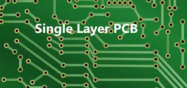
Single-Sided PCB Prototyping
One-sided PCBs include wiring and components on only one side of the board. This is the simplest form of PCB and is best used for straightforward circuits. One-sided prototyping is fast and inexpensive, but may not be appropriate for intricate designs with a lot of connections and components.
Double-Sided PCB Prototyping
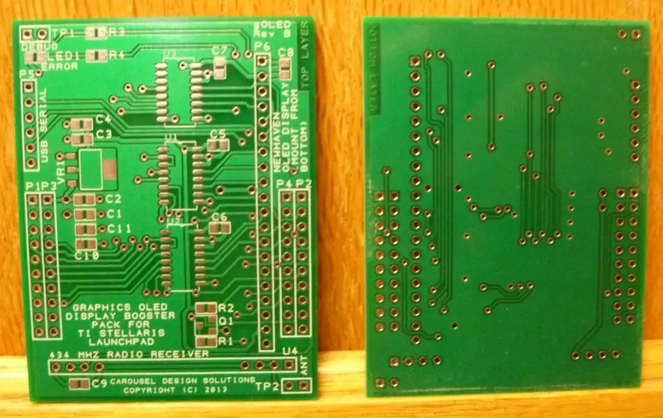
Double-sided PCBs have wiring and components on both sides of the board. Double-sided PCBs are used when a single-sided PCB just requires more complex circuit layouts and many components. Double-sided PCBs are more difficult to manufacture than single-sided PCBs, but may be required in more advanced designs.
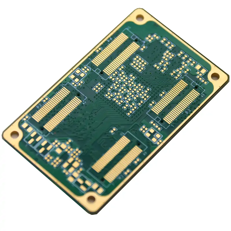
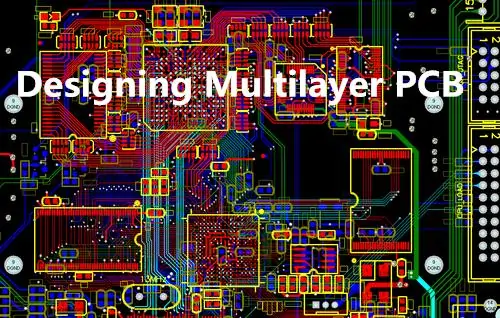
Multi-Layer PCB Prototyping
More complex designs use multilayer PCBs. Multilayer PCBs contain multiple layers of copper, and layers of insulation too. Multi-layer prototyping is required by high-density circuits used in smartphones, computers and other complex electronic devices. The process takes a lot of time and is expensive to make.
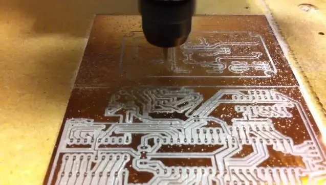
Using CNC Milling Machines
Another method that has been used in PCB prototyping is CNC (computer numerical control) milling. The process is carried out by using a machine that mills the PCB directly from the substrate of the copper foil. It is a general process used for rapid creation of prototypes in order to steer clear of chemical etching. This is, however, longer and less accurate compared to traditional methods.
3D Printing for PCBs
The 3D printing technology is applied for PCB prototyping in broader extent. The process prints one layer of material to create a structure of a PCB. It is relatively new technology and continuously developing, but can facilitate rapid prototyping with less cost and complexity.
Materials Used in PCB Prototyping
The PCB prototyping process is made with materials that have significant impacts on the board's performance and reliability. The most common materials are:
- Copper Clad Laminate: The raw material of most PCB. It is usually a thin copper coating applied over a fiberglass or plastic substrate.
- Solder Mask: Provides protection against short circuiting by coating the copper wires.
- Silkscreen Ink: Silkscreen ink is applied to print letters and symbols onto the board and aid in identifying parts.
- Drill Bits: Drill bits are utilized to make holes for component leads and via.
Challenges in PCB Prototyping
PCB prototyping is an important phase of the designing process, but the following are issues:
- Time Constraints: Depending on complexity, prototyping consumes more time, especially in the case of advanced PCBs.
- Cost: Prototyping for special substrates or multi-layer in general is expensive. However, the cost of errors after large-scale production is normally less.
- Design Errors: Good planning can result in design errors and can require numerous iterations to be corrected.
Conclusion
PCB prototyping is an indispensable process in electronic product development to guarantee that the design performs as planned before mass production. An understanding of the basics of PCB prototyping (design to test) will improve electronic product quality and efficiency. From simple circuits to complex multilayer substrates, prototyping saves time and money by catching errors early. Using proper materials and methods and having knowledge about the process is what guarantees that the PCB design works to specifications and functions properly with the final product.


 PCB AssemblyHRPCBA is a PCBA China manufacturer offering high-quality PCB assembly services with full-process support, from design to assembly and testing.
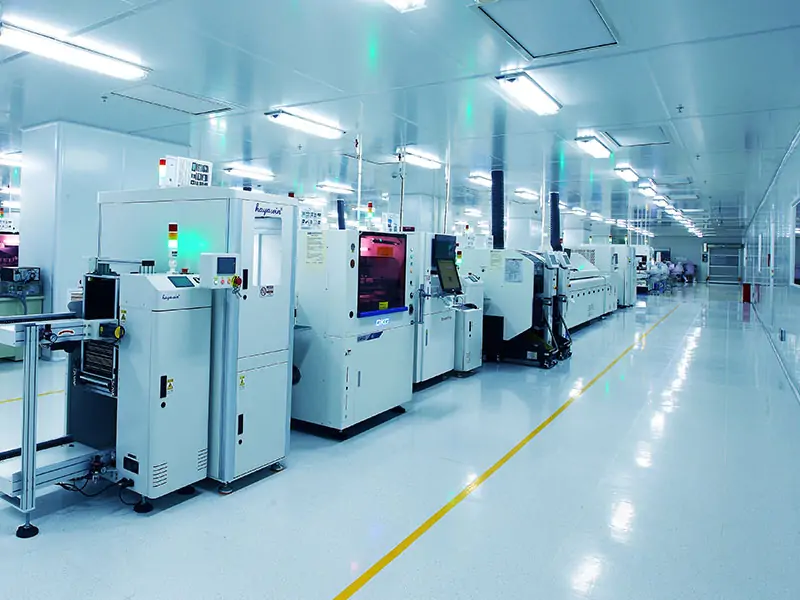 PCB ManufacturingHRPCBA is a leading PCB board manufacturer offering precision PCB fabrication services. Get high-quality boards with fast turnaround and competitive pricing
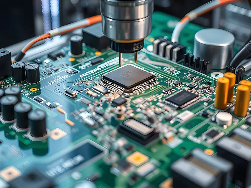 CapabilitiesDiscover HRPCBA’s robust PCB capabilities in custom PCB manufacturing services, where we transform your ideas into high-quality, functional circuit boards.