In PCB manufacturing, some processes may not appear on the finished circuit board, yet they can have a direct impact on manufacturing accuracy. Tooling pins are one of these often-overlooked details.
When people hear the term “tooling pin process,” they may assume it refers to a separate PCB manufacturing process. In practice, it is more closely related to Tooling Pins, Registration Pins, and Tooling Holes, which form part of a PCB positioning system.
Simply put, tooling pins work with tooling or registration holes to keep the PCB, inner layers, stencils, or production fixtures accurately positioned during manufacturing.
This becomes particularly important for multilayer PCBs, high-density boards, and SMT assembly. Even a small positional deviation between layers or during assembly can affect drilled holes, traces, pads, and component placement. Therefore, a seemingly simple positioning step can have an impact on the stability of the entire manufacturing process.
1. Why Are Tooling Pins Needed in PCB Manufacturing?
A PCB is not manufactured in a single step. Depending on the board structure and production requirements, the manufacturing process may involve inner-layer fabrication, lamination, drilling, plating, solder mask application, surface finishing, routing, and finally SMT assembly.
These processes have one common requirement: the PCB must have a reliable reference position throughout production.
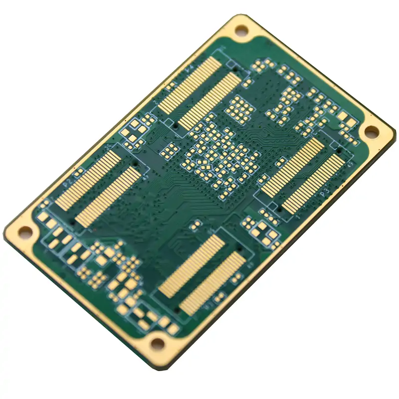
The basic purpose of a tooling pin is to establish a stable mechanical positioning reference. Tooling holes are normally designed in the PCB or production panel, allowing tooling pins to hold the board or material in a defined position.
This is particularly important for multilayer PCBs. The inner layers need to be aligned according to the designed stack-up before lamination. If different layers shift significantly, the relationship between drilled holes, inner-layer pads, and traces may be affected.
In other words:
The tooling hole provides the positioning reference, while the tooling pin engages with the hole to hold the PCB or material in position.
It is important to note that modern PCB manufacturing does not rely exclusively on traditional mechanical positioning. As manufacturing equipment has become more automated, optical alignment and machine vision have also become widely used. Mechanical positioning and optical alignment are often complementary rather than mutually exclusive.
2. Where Are Tooling Pins Used?
The importance of tooling pins does not come from their complexity. It comes from their ability to support accurate positioning across different manufacturing stages.
2.1 Multilayer PCB Layer Alignment
One of the typical applications of tooling pins is multilayer PCB fabrication.
During multilayer PCB manufacturing, inner-layer cores, copper foils, and prepreg materials are stacked according to the designed stack-up. In some traditional or specific lamination processes, precision tooling systems and tooling pins are used to hold the inner-layer materials in their intended positions before lamination.
This method is commonly referred to as pin lamination.
However, tooling pins alone cannot eliminate every source of layer-registration error. Material expansion and contraction, resin flow, thermal effects, and pattern compensation can also influence final registration accuracy.
Therefore, layer registration in PCB manufacturing is a comprehensive engineering issue rather than something that can be solved by positioning hardware alone.
2.2 PCB Machining and Fixture Positioning
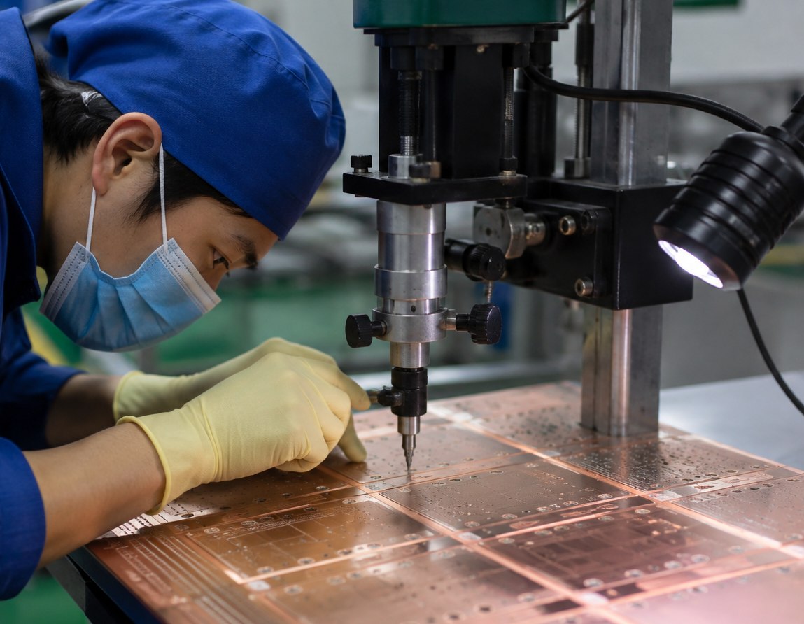
During processes such as drilling, routing, profiling, and certain testing operations, the PCB also needs to be accurately secured in equipment or fixtures.
If the PCB is loaded in a slightly different position every time, the same machine program can still produce positional variations in drilled holes or board outlines.
Tooling holes can therefore help establish a repeatable machining reference.
Several terms should be clearly distinguished:
-
Tooling Hole: Used primarily for mechanical positioning.
-
Mounting Hole: Generally intended for mounting the finished PCB into a product or enclosure.
-
Fiducial: An optical reference mark used by vision systems.
These features may sometimes look similar, but their functions are different.
2.3 PCB Positioning During SMT Assembly
The importance of positioning does not disappear after PCB fabrication.
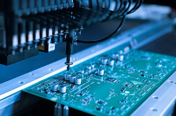
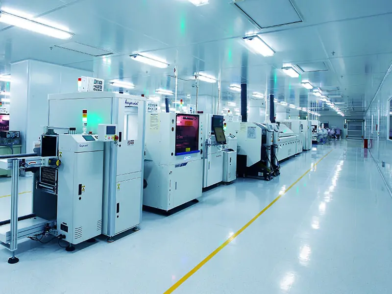
During SMT production, the PCB may go through solder paste printing, component placement, reflow soldering, and inspection processes. The board must remain accurately positioned so that stencil openings, PCB pads, and placement coordinates correspond correctly.
For example, during stencil printing, the stencil apertures must align accurately with the PCB pads. If the PCB is not positioned reliably, solder paste may be deposited incorrectly, potentially resulting in insufficient solder, solder bridging, or other printing-related defects.
Therefore, tooling holes, tooling pins, fiducials, and other positioning methods can all play important roles in SMT production. The actual method depends on the PCB design, equipment, fixture system, and manufacturer's process requirements.
For a broader overview of the SMT production process, you can also visit HRPCBA's SMT Assembly service page, which covers processes such as solder paste printing, component placement, reflow soldering, AOI, and X-ray inspection.
3. What Is the Difference Between Tooling Pins, Tooling Holes, and Fiducials?
These three terms often appear together in PCB manufacturing and assembly, but they should not be treated as the same thing.
| Item |
Tooling / Registration Pin |
Tooling Hole |
Fiducial Mark |
| What it is |
A mechanical positioning component |
A positioning reference hole on the PCB |
An optical reference mark |
| Main purpose |
Holds the PCB in a defined position |
Provides a reference for mechanical positioning |
Provides a reference for vision systems |
| Positioning method |
Mechanical |
Mechanical |
Optical |
| Common applications |
Lamination, fixtures, assembly |
PCB manufacturing, testing, assembly |
SMT and automated vision systems |
| Part of the electrical function? |
No |
Generally no |
No |
A simple way to understand the difference is:
Tooling pins answer “Where should the board be mechanically placed?” while fiducials help a vision system determine “Where is the board and how is it oriented?”
In automated production, these two positioning methods can also be used together.
4. What Should Be Considered When Designing Tooling Pins and Holes?
The positioning system may look simple, but once a PCB enters mass production, dimensions, tolerances, and locations can all affect performance.
4.1 Match the Tooling Hole and Tooling Pin
The tooling pin and tooling hole need to be properly matched.
The goal is not simply to make the fit as tight as possible. If the clearance is too small, insertion may become difficult and could potentially damage the hole or fixture. If the clearance is too large, positioning repeatability may be reduced.
4.2 Consider the Location of Tooling Holes
Tooling holes should be positioned according to the PCB dimensions, equipment structure, and fixture requirements.
They should provide a stable reference while also considering:
-
PCB edge clearance
-
Component placement
-
Copper and routing areas
-
Panelization
-
Routing or V-cut
-
Fixture support
-
Testing requirements
For production panels, the positioning holes may be placed in the panel frame rather than in the functional area of the PCB, depending on the manufacturing and assembly requirements.
4.3 Do Not Simply Copy a “Universal” Hole Size
There is no single tooling-hole size that is suitable for every PCB project.
Different PCB manufacturers, SMT machines, stencil systems, test fixtures, and positioning standards may use different requirements.
For this reason, a better approach is to confirm the manufacturer's and equipment's process requirements before finalizing tooling-hole dimensions, locations, and tolerances.
For high-density, multilayer, or HDI PCBs, positioning requirements should ideally be considered during the DFM review rather than being addressed only after production begins.
5. Why Can a Small Tooling Pin Affect PCB Quality?
The real challenge in PCB manufacturing is often not one individual process, but whether multiple processes can maintain consistent positioning from one stage to another.
From inner-layer fabrication and lamination to drilling, outer-layer processing, and SMT assembly, every stage involves positional relationships.
A reliable positioning system helps maintain a stable and repeatable manufacturing reference.
If positioning accuracy is compromised, the effects can potentially accumulate:
Positioning deviation → Layer registration variation → Changes in hole-to-pad alignment → Reduced manufacturing margin → Increased assembly difficulty
For conventional PCB designs, a certain amount of positional variation may remain within the acceptable manufacturing tolerance. However, high-density designs with fine traces, small pads, microvias, and tight geometries generally have less manufacturing margin, making registration and positioning control more important.
This is why PCB manufacturing quality is not determined only by material, copper thickness, trace width, or hole size. Reliable production also depends on positioning, alignment, manufacturing tolerances, material behavior, and the coordination between PCB fabrication and assembly.
Conclusion: A Small Tooling Pin Represents a Bigger Manufacturing Principle
The so-called “tooling pin process” is not a mysterious or independent PCB manufacturing technology. More accurately, it refers to the positioning work involving tooling pins, tooling holes, and related registration systems throughout PCB manufacturing and assembly.
The value of these components is not necessarily visible on the finished PCB. Their importance lies in helping the board maintain an accurate and repeatable position during different manufacturing operations.
For multilayer PCBs, high-density boards, and products requiring SMT assembly, reliable positioning and registration control are fundamental to manufacturing consistency.
For PCB projects, tooling holes and positioning requirements should ideally be considered during the design and DFM stages rather than being addressed only after production begins.
If you are looking for a one-stop solution covering PCB fabrication, component sourcing, SMT/THT assembly, and testing, you can also learn more about HRPCBA's Turnkey PCB Assembly service. HRPCBA provides PCB fabrication, component sourcing, assembly, and testing services, with manufacturing and assembly processes evaluated according to specific project requirements.
A small tooling hole may seem insignificant, but behind it is an important principle of PCB manufacturing: accuracy, repeatability, and process coordination.




 PCB AssemblyHRPCBA is a PCBA China manufacturer offering high-quality PCB assembly services with full-process support, from design to assembly and testing.
 PCB ManufacturingHRPCBA is a leading PCB board manufacturer offering precision PCB fabrication services. Get high-quality boards with fast turnaround and competitive pricing
 CapabilitiesDiscover HRPCBA’s robust PCB capabilities in custom PCB manufacturing services, where we transform your ideas into high-quality, functional circuit boards.