High frequency PCB design is an elaborate design and every manufacturing must be precise such that high speed signals flow can be handled. The use in communications equipment, radar systems, satellite technologies and other sophisticated electronic gear on which data must be relied to transmit swiftly with minimum interference and loss is the good use of these substrates. To design reliable substrates for such applications, the right material selection, the right layer configuration, and accurate impedance control are critical. This article explains key factors to consider when designing and assembling, explains the manufacturing process step-by-step, and introduces specialized services for producing reliable high frequency PCBs for demanding industrial and commercial applications.

What Should Be Paid Attention to When Producing and Assembling High-Frequency PCBs?
High-frequency PCB production differs from standard circuit board production due to the speed of signal transmission and sensitivity to interference. Here are the main factors to consider:
1. Material Selection
The requirement of special materials with low dielectric loss and stability of the performance are on high frequency signals. These substrates are not always satisfactory with FR4. Signal integrity is kept by Rogers, Teflon, or other high frequency laminating products. The chosen material should agree with the range of frequency of the device.
2. Controlled Impedance
High frequency PCB signal tracing should be designed to maintain consistent impedance. Impedance fluctuations cause reflection, noise and signal loss. These are achieved by controlling the width, interval and thickness of the dielectric layer between copper layers.
3. Layer Stack-Up
Multi-layer design is common in high frequency PCB. The arrangement of the signal layer, ground layer, and power layer is important for reducing electromagnetic interference and crosstalk. Properly planned stacking ensures stable performance even at very high frequencies.
4. Trace Routing
The length and the path of the trace has a direct influence on the performance in high frequency signals. The wiring has to be kept short and linear to reduce delays and losses. The sharp angles should be avoided and should have smooth curves to retain signal quality.
5. Solder Mask and Surface Finish
The choice of surface finish affects conductivity and soldering quality. ENIG (electroless nickel immersion gold) and HASL (hot air solder leveling) are common choices. Very high frequency PCBs recommend smooth surfaces and finishes that provide stable impedance.
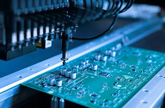
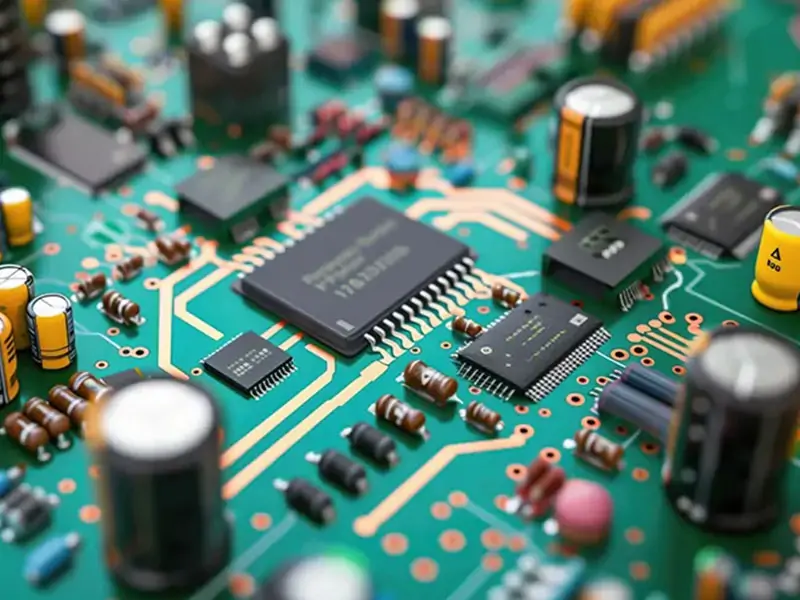
6. Assembly Precision
During assembly, placement of components and soldering should be precise without any superfluous parasite effects. Consistency and quality control are typically advised to be done with automatic assembly lines.
Describe the Production Process of High-Frequency PCBs
The manufacturing of high frequency PCBs involves several processes so that accuracy and performance is achieved. The following is an outline of the process:
1. Design and Layout
The initial process is the circuit design based on special software. Trace width, layer stacking and impedance control parameters are set by designers. The behavior of signals is often verified by using simulation tools prior to manufacturing.
2. Material Preparation
Proper board material is identified with respect to design requirements. This step matters since the dielectric characteristics of the material influence the overall performance of the high frequency PCB.
3. Inner Layer Processing
The circuit design is transferred to the copper plate by photoresist and exposure to UV light to produce the inner layer of the board. Unwanted copper is removed through etching leaving only what is necessary in the form of a trace.
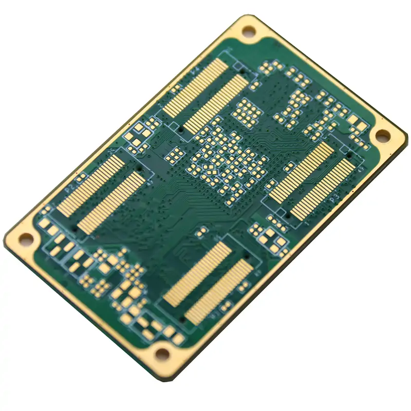
4. Lamination
In the case of multi-layer high-frequency PCB, the prepared inner layer is superimposed together with the insulation and bonded with heat and pressure. This produces a board with good rigidity and good layer-to-layer alignment.
5. Drilling and Plating
CNC machines and laser drills are used to drill holes to accommodate via and component pins. These holes are copper plated so that there is a proper electrical connection between the layers.
6. Outer Layer Imaging and Etching
The outer layer is treated together with the inner layer in the same process and the final circuit pattern is fixed. There must be high precision in order to keep the impedance and wiring dimensions within design specifications.
7. Surface Finish Application
The copper pad that is exposed has a conductive and protective finish. High-frequency PCBs are sought after to give smooth and flat surfaces to ensure that the electrical characteristics are kept constant.
8. Solder Mask and Silkscreen
Copper trace is covered with solder mask layer to ensure that it is not covered in solder bridge during assembly. Label components are added by silk screen printing.
9. Testing
All high-frequency PCBs are electrically tested prior to shipment to ensure continuity, short circuit and impedance matching. This makes the board to be compliant with the requirements of high frequency performance.
10. Assembly
Parts are placed and soldered using automatic pick-and-place machines and reflow soldering. Care is taken to maintain alignment and avoid noise and interference.
Common Applications of High-Frequency PCBs
High frequency PCBs are used in all situations where fast and stable signal transmission is required. Key applications include:
Communication Systems
Communication devices such as routers, antennas, and base stations use high frequency PCBs to achieve efficient data transfer and low signal loss.
Radar and Satellite Devices
The Redar and satellite technology rely on stable high speed signals. The high data rates can be supported by high frequency PCBs, which makes them suitable in such devices.
Medical Equipment
Diagnostic and imaging devices use high frequency PCB design to avoid distortion of sensitive signals.
Automotive Electronics
High-frequency PCBs are also employed in advanced driver assistance systems (ADAS) and vehicle radar systems to enhance proper sensing and communication.
Key Challenges in High-Frequency PCB Design
High-frequency PCB design has several challenges. Knowing about these issues prevents manufacturing and use issues.
Signal Integrity
Signal integrity is significant in high frequency PCBs to have the correct communication between parts. The higher the speed, the more the signals are vulnerable to loss, distortion or reflection. The proper dielectric material, proper trace width, and impedance control along the design will help keep the signal clean and correct. Latency also needs to be reduced and overall board performance needs to be ensured by careful wiring and trace length minimization.
Electromagnetic Interference
Electromagnetic interference (EMI) can cause serious problems with high frequency PCBs by blocking signal transmission. High-speed signals can generate noise that affects tracing and components around them. To minimize EMI, designers adopt appropriate grounding technology, shielding, and signal layer separation. Proper positioning of components and ground planes will allow you to keep the signals stable and limit unwanted interference when running on sensitive equipment.
Thermal Management
High-frequency PCBs and high-speed circuits produce a lot of heat when in operation, something that may influence component damage and signal performance. Thermal management involves temperature management of the product by use of thermal vias, copper plates and heat dissipation material. The layout that equally distributes heat is necessary to prevent hot spots and ensure reliability of the board, particularly in high-power devices that are constantly on.
Services We Provide for High-Frequency PCB Manufacturing
High frequency PCB production requires professional equipment and technology. We offer a comprehensive solution to meet your requirements:
One-Stop PCBA Manufacturing Services
We consistently respond to all processes from PCB manufacturing to final assembly. This reduces time and ensures quality control throughout the manufacturing process. Our team utilizes high frequency materials and advanced manufacturing technologies to provide reliable substrates.
OEM Services
We provide OEM manufacturing services for companies requiring their own brands. If you provide the design, we will manufacture high frequency PCB to meet the specifications and thoroughly maintain confidentiality.
ODM Services
If you need design or development support, we support concept creation, circuit design, and final manufacturing with ODM service. We optimize and develop high frequency PCB according to your request.
Sample Customization
We provide prototype and sample customization services to support pre-production design verification. This allows high-frequency PCBs to meet performance requirements and be adjustable at the initial stage of the process.
Conclusion
In designing and manufacturing high frequency PCBs, thorough attention to materials, layout and manufacturing processes is essential. From impedance control to precise assembly, each stage directly affects signal integrity and overall performance at high frequencies. Careful planning ensures that the board operates reliably in advanced communication, radar and electronic systems. In addition to our complete one-stop PCBA manufacturing service, OEM, ODM and sample customization services provide the necessary support to create high quality substrates. Specialized knowledge and advanced manufacturing methods enable high-frequency PCB design to be a reliable product for demanding industrial and commercial applications.


 PCB AssemblyHRPCBA is a PCBA China manufacturer offering high-quality PCB assembly services with full-process support, from design to assembly and testing.
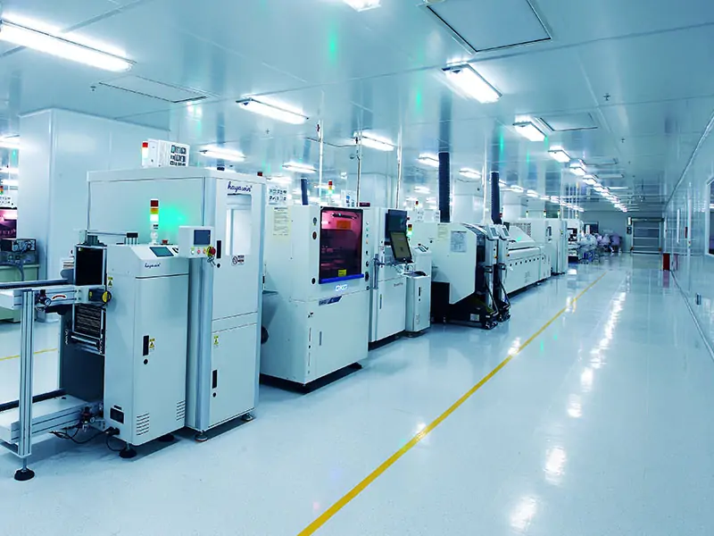 PCB ManufacturingHRPCBA is a leading PCB board manufacturer offering precision PCB fabrication services. Get high-quality boards with fast turnaround and competitive pricing
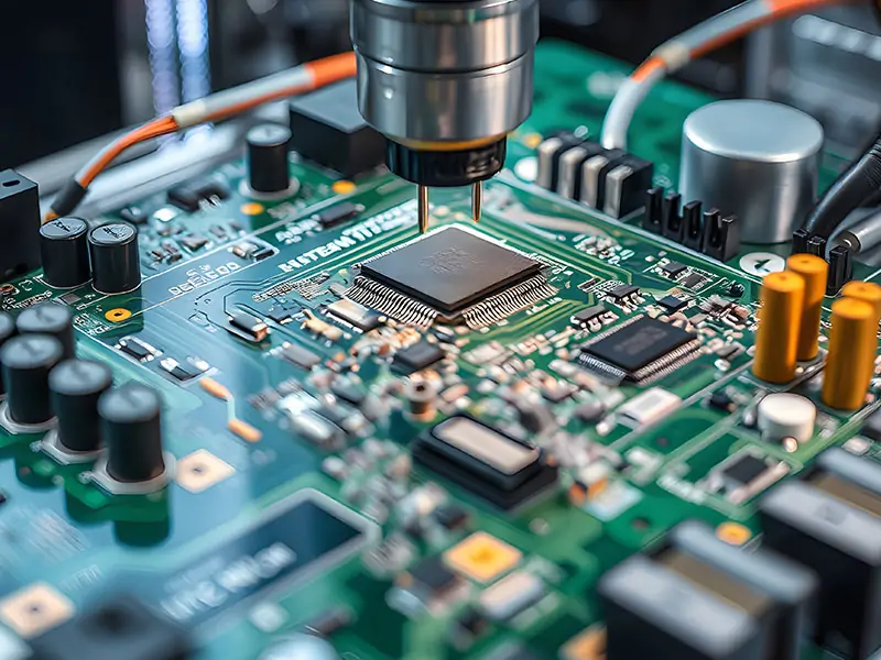 CapabilitiesDiscover HRPCBA’s robust PCB capabilities in custom PCB manufacturing services, where we transform your ideas into high-quality, functional circuit boards.