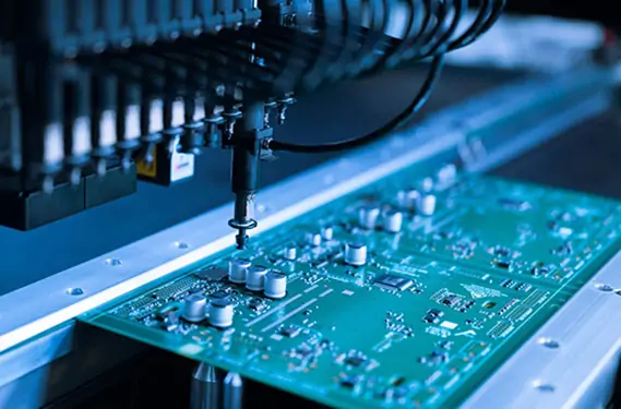
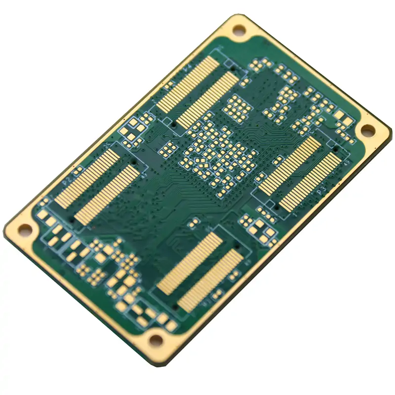
If you have ever prepared a PCB project for manufacturing, you have probably asked a simple question: What file type is used for PCB designs?
The answer is not just one file extension.
A PCB project usually generates several types of files as it moves from circuit design to board fabrication and assembly. The files used by the engineer during the design stage are often different from the files sent to the PCB factory. Once component assembly is involved, another set of data may be required.
For example, you might have an editable schematic and PCB layout on your computer, but the manufacturer may mainly work with Gerber files, drill data, fabrication notes, and other production documents. For SMT assembly, the BOM and component placement data become equally important.
Knowing what these files do—and when they are needed—can save a surprising amount of time when a design is ready to move into production.
PCB Design Files: From Schematic to Manufacturing Data
The easiest way to understand PCB file types is to follow the normal development process.
It usually starts with the circuit schematic.
A schematic file shows the electrical relationships between components. It tells you what is connected to what: power rails, signal nets, resistors, capacitors, ICs, connectors, and so on.
At this stage, the physical shape of the PCB is not the main concern. A resistor may be connected to a microcontroller in the schematic, but the schematic does not decide where that resistor will sit on the finished board.
Once the circuit is ready, the design moves into the PCB layout stage.
The PCB layout file contains the physical design of the board. This is where the circuit becomes an actual PCB. The designer places components, routes copper traces, creates pads and vias, defines the board outline, and prepares the required layers.
A layout file can contain a large amount of information, including:
These schematic and layout files are normally editable source files. Their exact format often depends on the PCB design software used to create them.
That is one reason why a PCB manufacturer may not necessarily ask for the original design file. In many cases, production data is exported from the layout software in a format that is easier to process during fabrication.
If you are working through the early stages of a new board, HRPCBA also provides a practical guide on" How to Design PCB", covering the broader process from design preparation to manufacturing.
Gerber and Drill Files: The Data Used for PCB Fabrication
When people talk about PCB manufacturing files, Gerber is usually one of the first formats mentioned.
Gerber data is widely used to communicate the graphical information needed to manufacture a PCB. Instead of sending one complete visual representation of the board, the design is generally separated into different layers.
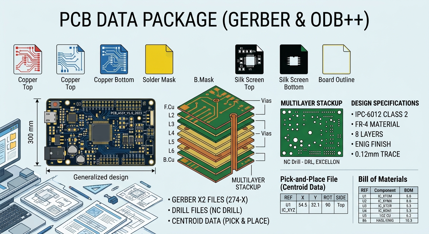
A typical Gerber package might contain separate files for the top copper, bottom copper, inner layers, solder mask, silkscreen, and board outline.
For a simple two-layer board, the file package may be relatively small. A multilayer PCB will naturally contain more manufacturing layers and therefore more data.
Drill information is also needed.
A drill file provides information about holes in the PCB, including their locations and sizes. These holes may be used for through-hole components, vias, mounting features, or other mechanical purposes.
Gerber and drill files are central to the PCB fabrication process, but they do not always cover every manufacturing requirement.
Some projects also require additional information, such as:
-
PCB material requirements
-
Finished board thickness
-
Copper thickness
-
Surface finish
-
Controlled impedance requirements
-
Stack-up information
-
Special routing or mechanical instructions
This is particularly important for complex or high-performance designs. A manufacturer should not be expected to guess requirements that are not included in the production data.
What Files Are Needed for PCB Assembly?
Fabricating a bare PCB is only one part of the job.
If components need to be mounted onto the board, the assembly process requires more information.
The most common document is the Bill of Materials, or BOM.
A BOM identifies the components used in the design. Depending on how it is prepared, it may include reference designators, quantities, part numbers, descriptions, package information, and other sourcing details.
A clean BOM can make the sourcing process much easier. On the other hand, unclear component information can slow things down. A description such as “10k resistor” may not be enough if there are specific package, tolerance, or other requirements that affect the final assembly.
Another important file is the Pick-and-Place file, sometimes referred to as centroid data or component position data.
This file helps automated assembly equipment identify where each component should be placed. It commonly includes:
-
Reference designator
-
X and Y coordinates
-
Rotation
-
PCB side
Although the data may look straightforward, it should still be checked. Different PCB design tools and assembly systems can use different coordinate origins and rotation conventions.
For that reason, assembly data should be reviewed together with the PCB layout and BOM rather than treated as an isolated file.
The table below gives a quick overview of the most common PCB design and production files.
| File Type |
What It Is Used For |
Typical Stage |
| Schematic File |
Defines electrical connections between components |
Circuit Design |
| PCB Layout File |
Contains the editable physical PCB design |
PCB Layout |
| Gerber File |
Provides layer data for PCB fabrication |
PCB Manufacturing |
| Drill File |
Defines hole locations and sizes |
PCB Manufacturing |
| BOM |
Lists components required for assembly |
Component Sourcing |
| Pick-and-Place File |
Provides component position and rotation data |
SMT Assembly |
| Assembly Drawing |
Helps clarify placement and assembly details |
PCB Assembly |
What Should You Send to a PCB Manufacturer?
The answer depends on what you want the manufacturer to do.
If you only need a bare PCB, the main requirement is a complete fabrication data package. This commonly includes Gerber files, drill data, and any technical specifications that are not clearly defined in the graphical data.
If you need a complete PCBA service, more information is usually required.
A typical assembly package may include the PCB fabrication data, BOM, Pick-and-Place file, assembly drawings, and any special production or testing instructions.
One thing worth checking before sending the files is whether everything belongs to the same design revision.
This sounds obvious, but version mismatches are a common source of problems. The Gerber files may have been updated while the BOM was not. The PCB layout may be revision B, while the Pick-and-Place file still belongs to revision A.
Before submitting a project, check that:
-
All files come from the latest approved design revision.
-
The PCB outline is clearly defined.
-
Required fabrication layers are included.
-
Drill data matches the PCB design.
-
The BOM matches the latest schematic and layout.
-
Component placement data has been exported correctly.
-
Special manufacturing requirements are documented separately when necessary.
For customers who need both PCB fabrication and assembly, HRPCBA.COM provides integrated PCB and PCBA manufacturing services. A complete and well-organized data package can make engineering review and production preparation more efficient.
Final Thoughts
So, what file type is used for PCB designs?
In real projects, the answer is usually several file types rather than one.
The schematic and PCB layout are the main design files.
Gerber and drill files are commonly used to transfer PCB fabrication data.
For assembly, the BOM, Pick-and-Place file, and assembly documentation provide the information needed to source and place components.
The file extension itself is not the most important part.
What matters is whether the information is complete, consistent, and suitable for the next stage of the project.
A well-prepared PCB package makes it easier for engineers and manufacturers to review the design. It also reduces the risk of working with outdated files, missing layers, incorrect drill data, or inconsistent assembly information.
Before releasing a project for production, take a few minutes to check the data package as a whole—not just one file at a time. That simple step can prevent unnecessary questions later and help the project move more smoothly from PCB design to fabrication and assembly.
For more information about PCB manufacturing and assembly services, visit HRPCBA.COM.
FAQ
Q: What is the most common file used for PCB manufacturing?
A: Gerber files are widely used to communicate PCB layer information for fabrication. Drill data and additional manufacturing requirements may also be needed.
Q: Do I need to send the original PCB design file?
A: Not always. Production-ready fabrication and assembly files are often sufficient. However, native design files may be useful if additional engineering review or design changes are required.
Q: What files are needed for PCB assembly?
A: A typical PCB assembly project may require PCB fabrication data, a BOM, Pick-and-Place data, assembly drawings, and any special manufacturing or testing instructions.
Q: Can a PCB manufacturer work from a PDF?
A: A PDF can be useful as a reference, but it usually does not contain enough structured information for PCB fabrication or automated assembly. Production data should normally be provided in the appropriate manufacturing formats.




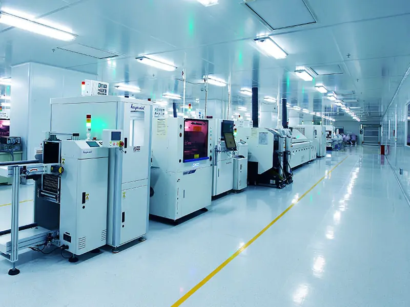
 PCB AssemblyHRPCBA is a PCBA China manufacturer offering high-quality PCB assembly services with full-process support, from design to assembly and testing.
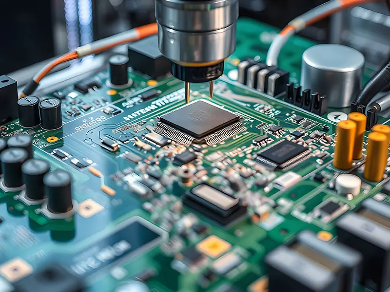
 PCB ManufacturingHRPCBA is a leading PCB board manufacturer offering precision PCB fabrication services. Get high-quality boards with fast turnaround and competitive pricing
 CapabilitiesDiscover HRPCBA’s robust PCB capabilities in custom PCB manufacturing services, where we transform your ideas into high-quality, functional circuit boards.