Introduction: Understanding PCB Fabrication and Assembly
PCB fabrication and PCB assembly are two essential stages in electronic manufacturing. Although both involve printed circuit boards, they serve different purposes and require different production processes.
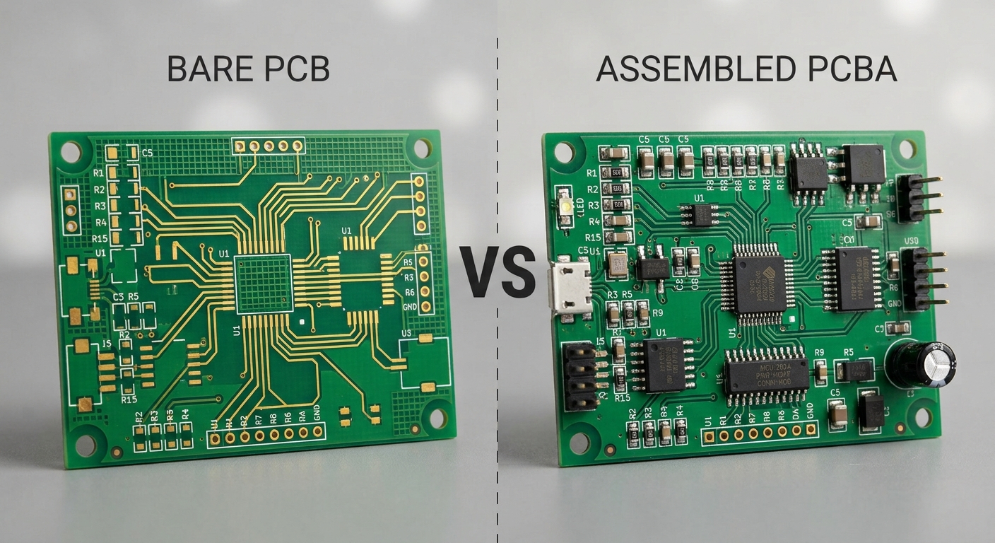
In simple terms, a PCB fabricator produces the bare circuit board, while a PCB assembler installs electronic components onto that board to create a finished printed circuit board assembly (PCBA).
For electronics engineers, product developers, and purchasing teams, understanding this distinction is important when selecting manufacturing partners. Choosing the wrong type of supplier may lead to unnecessary communication, production delays, or difficulties when coordinating different manufacturing stages.
So, what exactly does a PCB fabricator do, and how is its work different from that of a PCB assembler? Let's take a closer look at their processes, equipment, and responsibilities.
What Does a PCB Fabricator Do?
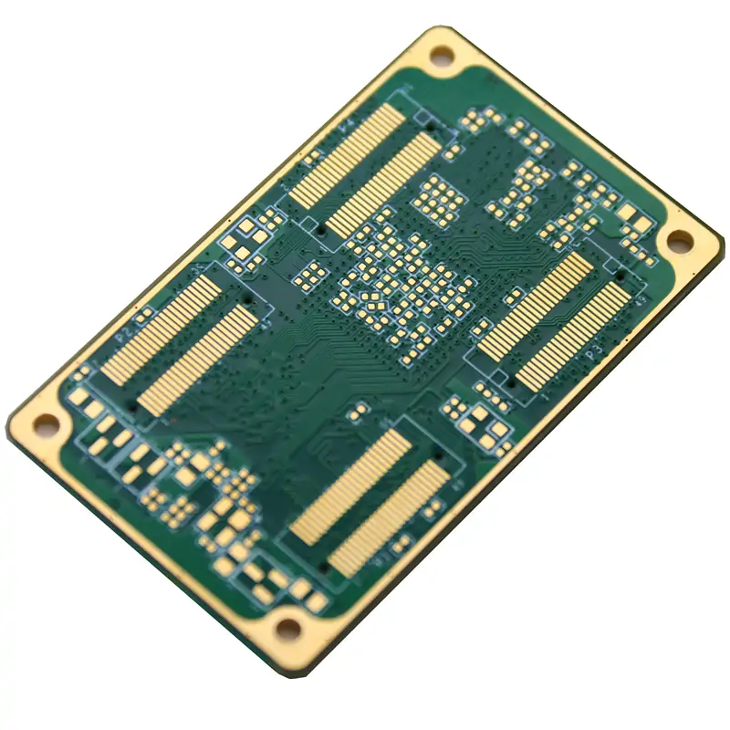
A PCB fabricator is responsible for manufacturing bare printed circuit boards based on customer design files. At this stage, the board does not yet contain electronic components such as resistors, capacitors, or integrated circuits.
The manufacturer's job is to turn the design data into a physical board with the required circuit patterns, dimensions, layer structure, and electrical connections.
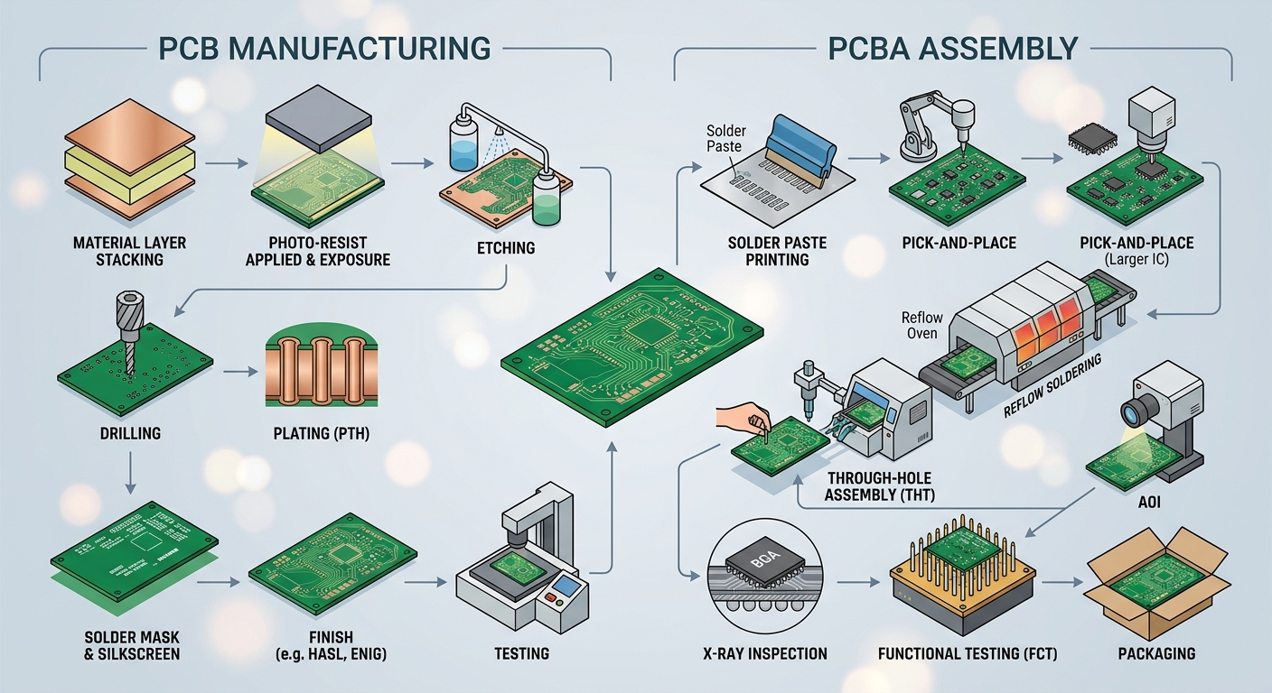
The main PCB fabrication processes include the following.
1. Material Preparation
The first step is selecting the appropriate base material according to the board's design and application.
Common materials include FR-4, aluminum-based materials, and specialized high-frequency laminates. Each material has different electrical, thermal, and mechanical properties. The choice depends on factors such as operating temperature, signal requirements, mechanical strength, and cost.
2. Circuit Pattern Formation
Circuit pattern formation is one of the most important stages in PCB manufacturing.
Using manufacturing data such as Gerber files, the fabricator transfers the designed circuit patterns onto copper-clad laminate. Processes such as imaging, developing, and etching are then used to form the required copper traces.
Trace width, spacing, and copper thickness all influence the electrical performance and manufacturing quality of the finished board.
3. Drilling and Plating
Drilling creates the holes required for component mounting and electrical connections between different PCB layers.
For multilayer boards, plated through-holes are particularly important. Copper plating on the hole walls creates electrical connections between the relevant copper layers.
Depending on the board structure, fabrication may also involve inner-layer processing, lamination, drilling, and outer-layer pattern formation.
4. Solder Mask and Surface Finishing
After circuit formation, a solder mask is applied to protect the copper traces and help prevent unwanted solder bridging during assembly.
The exposed copper pads then receive an appropriate surface finish. Common options include HASL and ENIG, depending on the board's requirements for solderability, storage, and application.
5. Inspection and Electrical Testing
Before delivery, the bare PCB needs to undergo inspection according to its specifications.
Typical checks may include visual inspection, dimensional verification, and electrical testing for open and short circuits. Additional inspection requirements depend on the board design and customer's quality standards.
The final product from a PCB fabricator is a bare circuit board, ready for the next stage of electronic assembly.
For more information about board types and manufacturing capabilities, visit our PCB Manufacturing page.
What Does a PCB Assembler Do?
Unlike a PCB fabricator, a PCB assembler focuses on installing electronic components onto manufactured bare boards. The goal is to turn an unpopulated PCB into a functional PCBA.
This process involves more than simply placing components. It also includes soldering, inspection, and, when required, electrical and functional testing.
The main PCB assembly stages include:
1. Component Sourcing and Preparation
Before assembly begins, the required electronic components must be prepared according to the Bill of Materials (BOM).
A BOM typically identifies component part numbers, specifications, quantities, and other purchasing information. When the assembly supplier is responsible for sourcing, component specifications and supplier details also need to be checked.
Using the correct components is essential because incorrect or incompatible parts can affect both assembly quality and final product performance.
2. Solder Paste Printing
For surface mount technology (SMT), solder paste is first printed onto the designated PCB pads through a stencil.
The amount and position of the solder paste matter. Too much, too little, or poorly aligned paste may result in soldering defects during later stages.
3. Component Placement
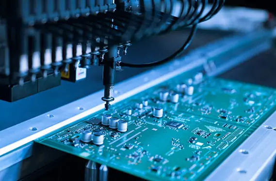
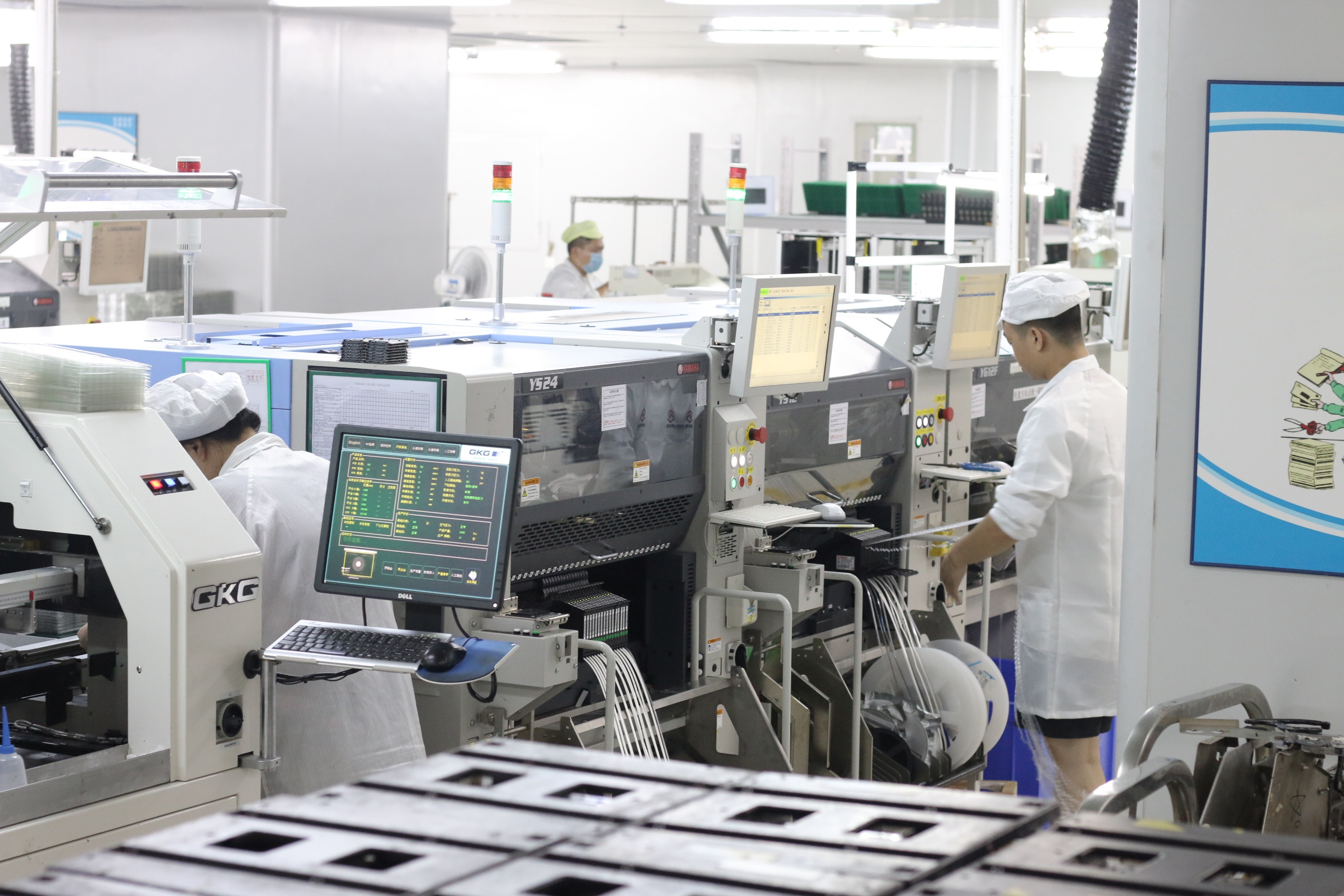
After solder paste printing, pick-and-place machines position surface-mount components according to the placement data and assembly instructions.
Resistors, capacitors, integrated circuits, and other components must be placed in their correct positions and orientations.
For high-density boards and miniature components, placement accuracy becomes particularly important.
4. Reflow Soldering and Through-Hole Assembly
Once the components are placed, the board typically passes through a reflow oven. The temperature profile melts the solder paste and forms electrical and mechanical connections between the components and PCB pads.
Some products also contain through-hole components. These require through-hole technology (THT) assembly, which may involve wave soldering, selective soldering, or manual soldering, depending on the design and production requirements.
This is why SMT is not the only assembly method used in PCBA manufacturing. Many products combine SMT and THT processes.
5. Inspection and Testing
After soldering, the assembled board needs to be inspected to check component placement, solder joints, and electrical performance.
Common inspection and testing methods include:
-
AOI (Automated Optical Inspection): Checks visible assembly defects, component placement, and orientation.
-
X-ray Inspection: Helps examine hidden solder joints, particularly those beneath BGA components.
-
ICT (In-Circuit Test): Checks electrical connections and selected component characteristics through test points.
-
Functional Testing: Verifies whether the assembled board operates according to its intended design.
Not every PCBA requires every testing method. The appropriate inspection plan depends on board complexity, component packages, product requirements, and the customer's quality standards.
The final output of a PCB assembler is a populated PCBA. Depending on the supplier's capabilities and project requirements, additional services may include programming, product-level assembly, and packaging.
You can learn more about these processes on our SMT Assembly page.
PCB Fabricator vs. PCB Assembler: What Are the Key Differences?
Although PCB fabricators and PCB assemblers both contribute to electronics manufacturing, their responsibilities, materials, equipment, and final products are different.
The following table summarizes the main differences.
| Comparison |
PCB Fabricator |
PCB Assembler |
| Main Responsibility |
Bare PCB manufacturing |
Electronic component assembly |
| Main Output |
Bare PCB |
PCBA |
| Main Materials |
Copper-clad laminate, copper foil, prepreg |
Bare PCBs, electronic components, solder paste |
| Main Processes |
Etching, drilling, plating, lamination |
SMT, THT, reflow soldering |
| Main Equipment |
Drilling machines, imaging systems, plating lines |
Stencil printers, pick-and-place machines, reflow ovens |
| Required Files |
Gerber files, drill files, stack-up information |
BOM, pick-and-place files, assembly drawings |
| Quality Inspection |
Electrical testing, dimensional and visual inspection |
AOI, X-ray, ICT, functional testing |
How Are PCB Fabrication and Assembly Connected?
Although these are two separate manufacturing stages, they are closely connected.
The bare board produced by a PCB fabricator provides the foundation for the assembly process. If the board has problems with pad dimensions, hole positions, surface finish, or manufacturing tolerances, these issues may affect component placement and soldering quality.
On the other hand, not every defect found during PCB assembly originates in the assembly process. Issues related to PCB design, board flatness, or manufacturing dimensions may also affect the final PCBA.
For this reason, communication between the fabrication and assembly teams is important. Reviewing design files, manufacturing requirements, and quality expectations before production can help reduce avoidable problems.
Which Service Should You Choose for Your Project?
After understanding the differences, the next question is which service your project actually needs.
The answer depends on your current production stage, available resources, and manufacturing requirements.
Scenario 1: You Only Need Bare PCBs
If you already have complete PCB design files and your company has its own component sourcing and assembly arrangements, PCB fabrication alone may be sufficient.
In this case, pay attention to material selection, layer count, board thickness, trace specifications, surface finish, and electrical testing.
A suitable fabricator should be able to manufacture the board according to the released design data and agreed specifications.
Scenario 2: You Already Have Bare PCBs
If your bare boards are ready but the components have not yet been installed, you need a PCB assembly service.
Commonly required files include:
For projects involving BGA packages, fine-pitch components, or high-density placement, it is also important to confirm that the assembler has the necessary equipment and process experience.
Scenario 3: You Need a Complete PCB and PCBA Solution
Some projects require more than bare board manufacturing or component assembly alone. They may involve PCB fabrication, component sourcing, SMT placement, THT assembly, inspection, and functional testing.
In this situation, a turnkey PCB assembly provider may be worth considering.
A one-stop manufacturing arrangement allows several connected processes to be coordinated through a single supplier. This can reduce communication between multiple vendors and simplify material transfers and production scheduling.
However, turnkey service is not automatically the best choice for every project. Buyers should still evaluate the supplier's technical capabilities, component sourcing process, quality management, production capacity, lead time, and overall cost.
For projects requiring both bare PCB production and PCBA assembly, working with a supplier that supports both processes can make manufacturing coordination more straightforward.
Conclusion
PCB fabricators and PCB assemblers perform different but closely related roles in electronic manufacturing.
A PCB fabricator produces the bare circuit board by converting design data into a physical PCB. A PCB assembler installs electronic components, completes the soldering process, and carries out the required inspections and tests to create a PCBA.
If a project only requires bare boards, a PCB fabricator may be all that is needed. If components need to be installed, a PCB assembly provider is required. For projects involving both processes, a supplier with integrated PCB manufacturing and assembly capabilities may offer a more coordinated production arrangement.
HongRong (Shenzhen) Electronics Co., Ltd. provides PCB manufacturing, component sourcing, SMT and THT assembly, and related testing services. Customers can explore these capabilities according to their individual project requirements.
Understanding the difference between PCB fabrication and PCB assembly is a practical first step toward choosing the right manufacturing partner and managing the journey from design to production more effectively.



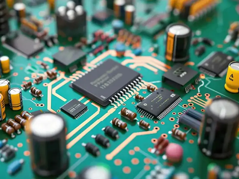 PCB AssemblyHRPCBA is a PCBA China manufacturer offering high-quality PCB assembly services with full-process support, from design to assembly and testing.
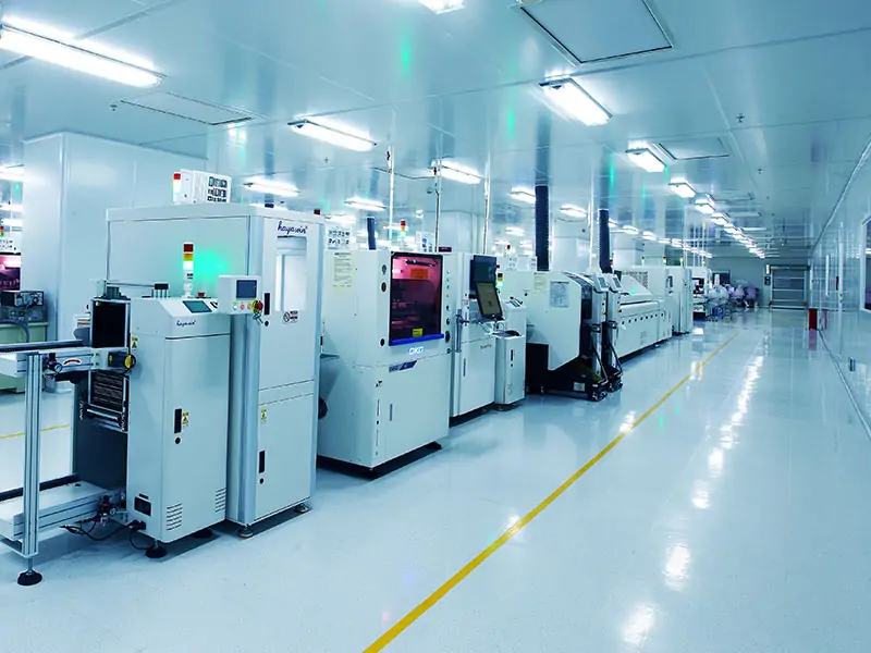 PCB ManufacturingHRPCBA is a leading PCB board manufacturer offering precision PCB fabrication services. Get high-quality boards with fast turnaround and competitive pricing
 CapabilitiesDiscover HRPCBA’s robust PCB capabilities in custom PCB manufacturing services, where we transform your ideas into high-quality, functional circuit boards.